I’m creating this post as a complimentary article to the discrete 7408 that I designed and am selling on my site.
I have always been fascinated how things work down the the absolute core. I was never just satisfied by asking the question, “How does an AND gate work?” and someone basically drawing the AND gate symbol with 2 inputs and an output and then stating that in order for you to have a hi output, you’ll need to have 2 hi inputs. That’s a very simplistic answer and would probably appease many but when I ask the question, “How does an AND gate work?”, what I mean is what are the components it would take to build one and don’t just throw a 7408 (Quad dual input AND gate IC at me) I want to know how these gates are constructed electronically.
In its simplest form, you could construct an and gate out of mechanical switches that you would manually flip on and off but that’s not what we want. We want an AND gate that is controlled by binary values 1 and 0, true and false, hi and lo, call them what you will, they all mean the same thing.
So if we want to build an electronic AND gate we will need electronic switches, and what would those look like? Well they come in the form of several semiconductors but for our purposes we will need transistors, specifically of the NPN variety. Something like a 2N3904 should do.
But how does a transistor work?
Well, the NPN transistor that we’re using has 3 pins. These are called the Colletor, Base and Emitter.
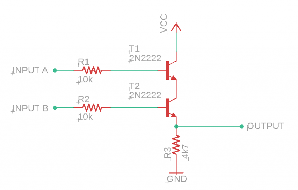
Applying a forward voltage at the Base of the transistor allows the current to flow to the emitter. If we were to connect 2 transistors in such a way that transistor 1 has its collector connected to +5V and its emitter connected to the collector of transistor 2 and transistor 2 has its emitter connected to ground through a pull down resistor then we could use the bases of each transistor as inputs and then use the emitter at transistor 2 as the output.
This would then become our AND gate because the bases at Transistor 1 and Transistor 2 must both be high in order for current to flow at the emitter of Transistor 2.
This can be represented in the following schematic diagram:
AND gates are part of the fundamental building blocks to designing electronic circuits. These, along with NOT, NAND, OR, NOR, XOR and several others can be used to build highly complex circuits. Granted, in this day and age you wouldn’t be using discrete 7408 IC’s to design your circuits with all of the SOC devices readily available it makes these older discrete logic IC’s sort of obsolete. Even still I don’t think they’ll be disappearing any time soon.
Hopefully this short little write up has helped you get a clearer understanding of how AND gates work in electronic circuits. If you haven’t had a chance yet to check out my “Giant” Discrete 7408 soldering kit then you’re missing out. Wether you are still learning about electronics and want to practice your soldering skills or you’re just a nerd like me who’d like to build one of these just for the fun of having it and maybe framing it then this is the perfect project for you.


0 Comments for “How do AND gates work?”