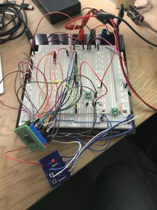
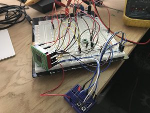
So recently I’ve been fascinated with with FPGA’s and what they have to offer. There almost seems to be an overwhelming amount of options out there and it may not always be obvious which FPGA you should choose. If you’re just starting out then a great choice is the iCE40HXK1-VQ100 which can be had from Mouser or any other distributor for around $5.00 which makes it one of the cheapest in the game.
Anyway, this post isn’t about that.
I have an Altera dev board, DE0-Nano which I used to build a prototype for a project that I’m working on.. Yes I know lots of great info there. More will be revealed in time.
Either way, the next step is to draw up the schematic and have a PCB manufactured but before doing so, I wanted to make sure that I completely understood everything that would be involved in designing this board. I wanted to build a comparable circuit on a breadboard as a proof of concept before designing something.
I picked up some generic breakout board from Amazon which came in handy are actually quite inexpensive. I soldered on the FPGA and some headers.
It took some time but I eventually was able to connect all of the required components to get this thing operational.
I’ll follow up this post eventually with a how to but for now I just wanted to show everyone that it is possible and that you can do this with a minimal set of components. You don’t even need an external oscillator if all you’re doing is just logic gates but that’s no fun. You’ll need to eventually connect an oscillator to do cool things.
Enjoy the pictures:


The 2nd picture is after I started eliminating unnecessary connections. I found out that you do not need to connect VCC_IO or GND pins on banks that you aren’t planning on using. You also don’t need all 4 core VCC connections. The only core VCC connections needed are on Bank1 and Bank2 which also required GND pins connected. I have .1uF capacitors connected between VCC and ground ( 1 for each VCC, VCC_IO, VPP_2V5 and SPI_VCC ) I have 1.2 V going to the core and 3.3 V to everything else.
For the AND gate, I’ve got 2 pull down resistors connected to pins 26 and 27 which I designated as output pins in the Verilog file. I’ve got pin 28 connected to the LED which is designated as an output.
Ok, if I write any more this will turn into a tutorial which was not my intention but I will eventually follow up with one.

0 Comments for “FPGA on a Breadboard – iCE40HXK1-VQ100”