Update – 2025.12.15
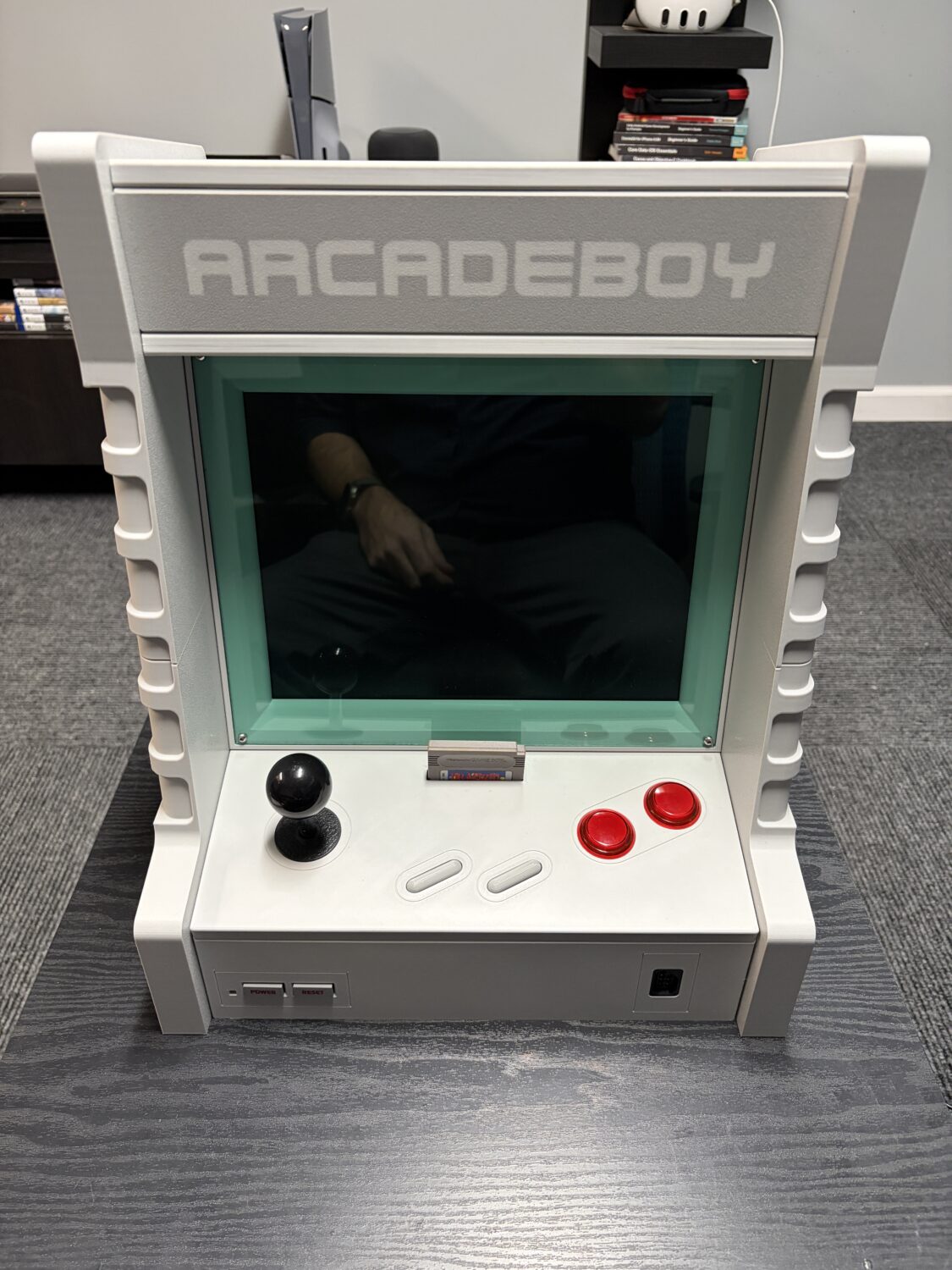
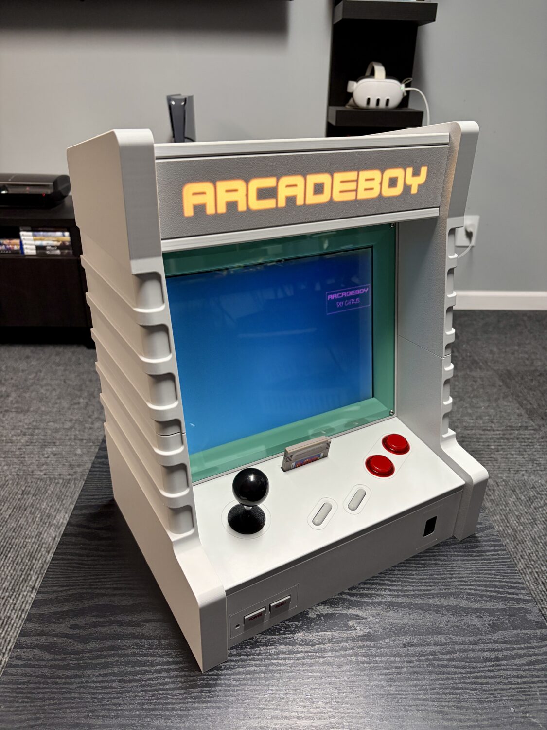
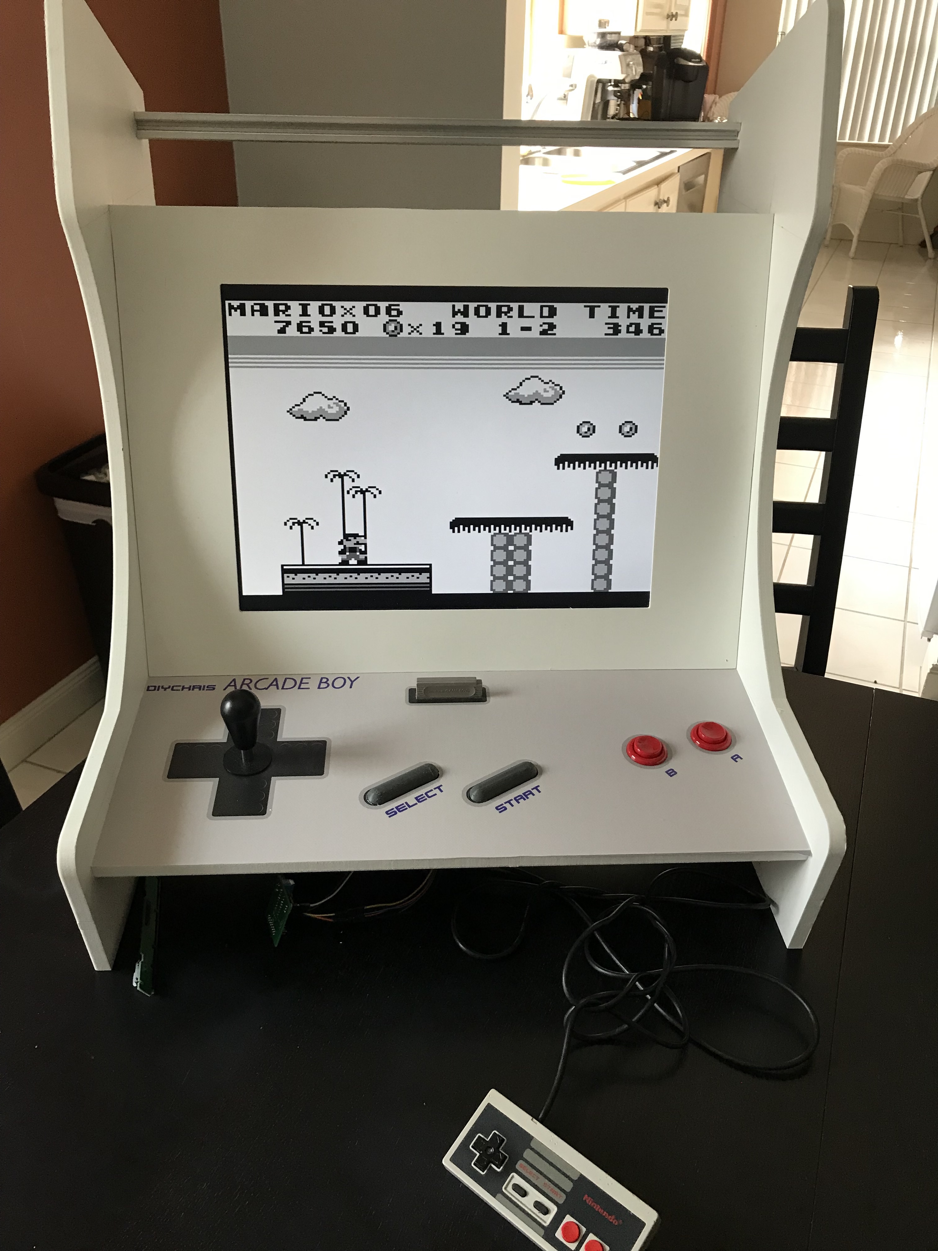
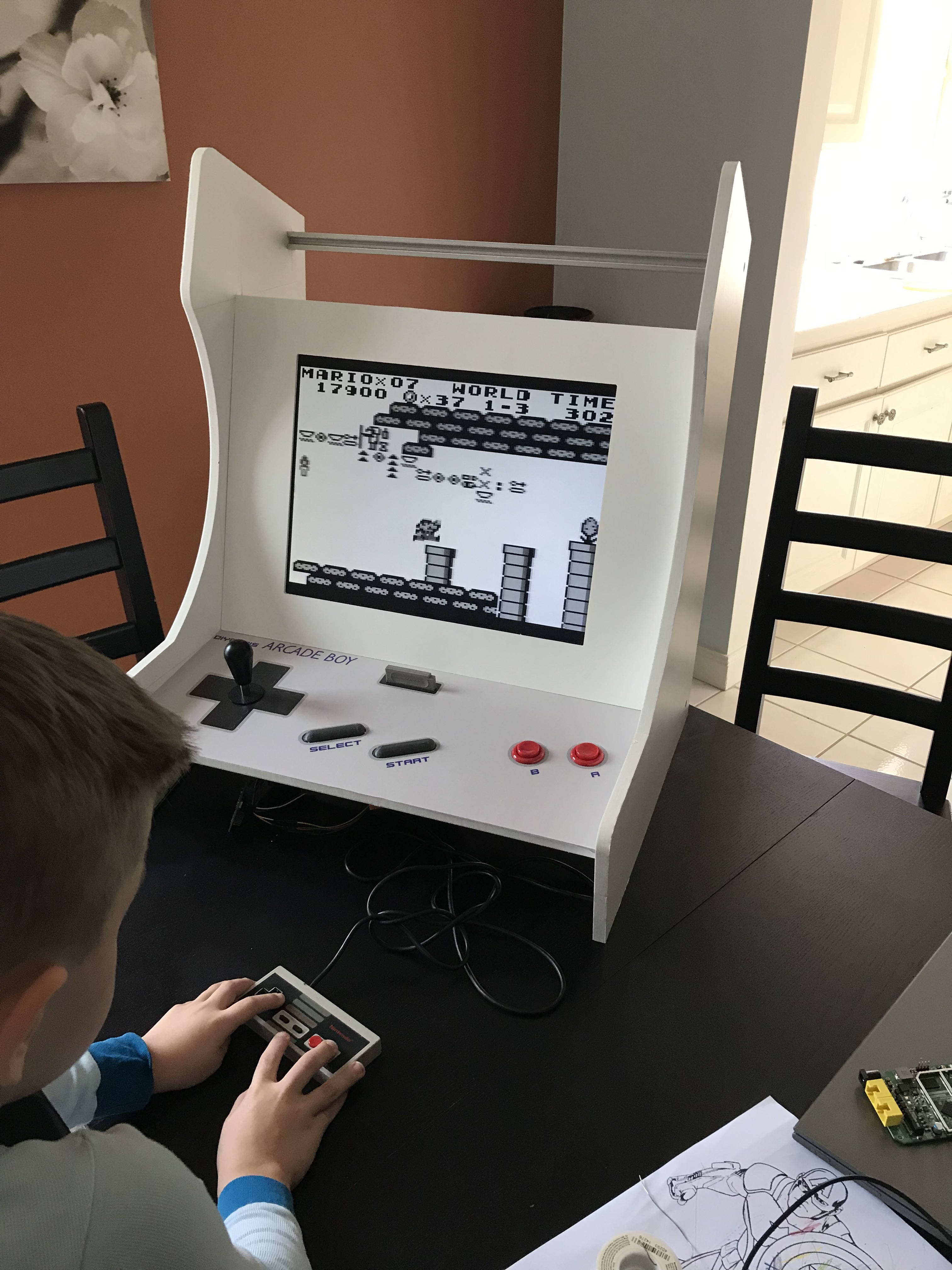
It’s been about 2 weeks since the last update and the project has made tons of progress. I’m now ready to share a sneak peak of what is close to the final design of the cabinet and how the ArcadeBoy will work but first some info.
Inside the ArcadeBoy lives an actual GameBoy (Original DMG-01) with its top removed. That’s the part with the screen in case you were wondering. Why remove this? The screen and input controls connect to the DMG via an FPC cable and I need all of these signals to pass along to the heart of ArcadeBoy, the custom FPGA driven mainboard I designed to drive the screen, and input controls.
The current firmware on the FPGA takes the input pixel data from the Gameboy and passes it along to the LCD panel while performing a 1:1 3x upscale. This means that the output from the GameBoy remains unaltered and is perfectly scaled and centered on an LCD panel at an 800×600 resolution. Why 800×600? Well, because much like the original GameBoy Kiosk I wanted a GameBoy bezel around the screen output so I needed space.
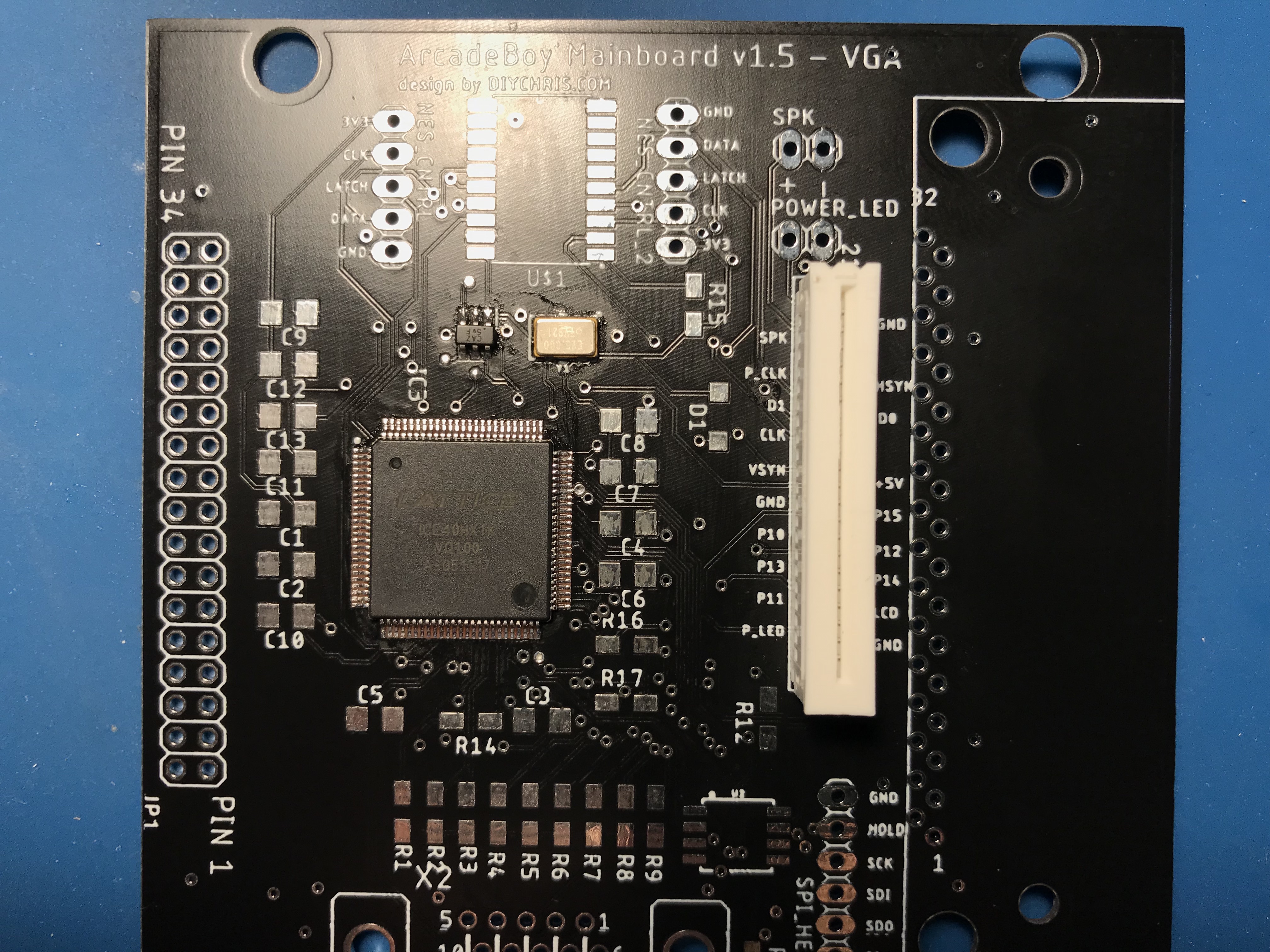
The original ArcadeBoy mainboard converted the digital pixel data to output over analog RGB so that you could plug in a VGA monitor which takes the VGA signal and converts it back to digital. That’s a whole lot of converting which is totally unnecessary so I eliminated the VGA output and decided to deliver a pure digital signal to the panel instead.
Right now I’m working on another revision to the mainboard that will allow for easy firmware updates for future enhancements / updates.
The plan is to offer ArcadeBoy in both a DIY Kit and a fully built version once it’s been thoroughly tested! I’m thinking about doing an initial launch on Kickstarter to gauge interest and to offer some special rewards to early bird supporters! Ok, that’s enough ranting, lets take a look at ArcadeBoy!
Update – 2025.12.04
Well here we are 6 years later. Man, it doesn’t feel like a whole 6 years has passed since my last update on this project. So much has happened since the original idea for the project.
So the reason for this latest entry was to give an update on this projects current status and plans going forward. Unfortunately, I haven’t made any progress on this iteration of the project. The design just didn’t feel right and continuing to use PVC board and a CNC to design the cabinet was a cumbersome process that would be difficult for anyone following this project to replicate.
With advancements in 3D printing, it is now possible to do some really great things. Sometimes it’s difficult to even discern if something was 3d printed or not. So maybe you’ll see where I’m going with this?
I recently started getting back into the nostalgia of retro gaming and was trying really hard to locate a Gameboy Kiosk, with no luck. Not to mention, if I would have been able to find one it would have been well outside of my price range.
I decided instead that I was going to go back to my original idea, ArcadeBoy and re-design the cabinet from scratch inspired by the Gameboy Kiosk along with a complete re-design of the mainboard that drives the LCD panel.
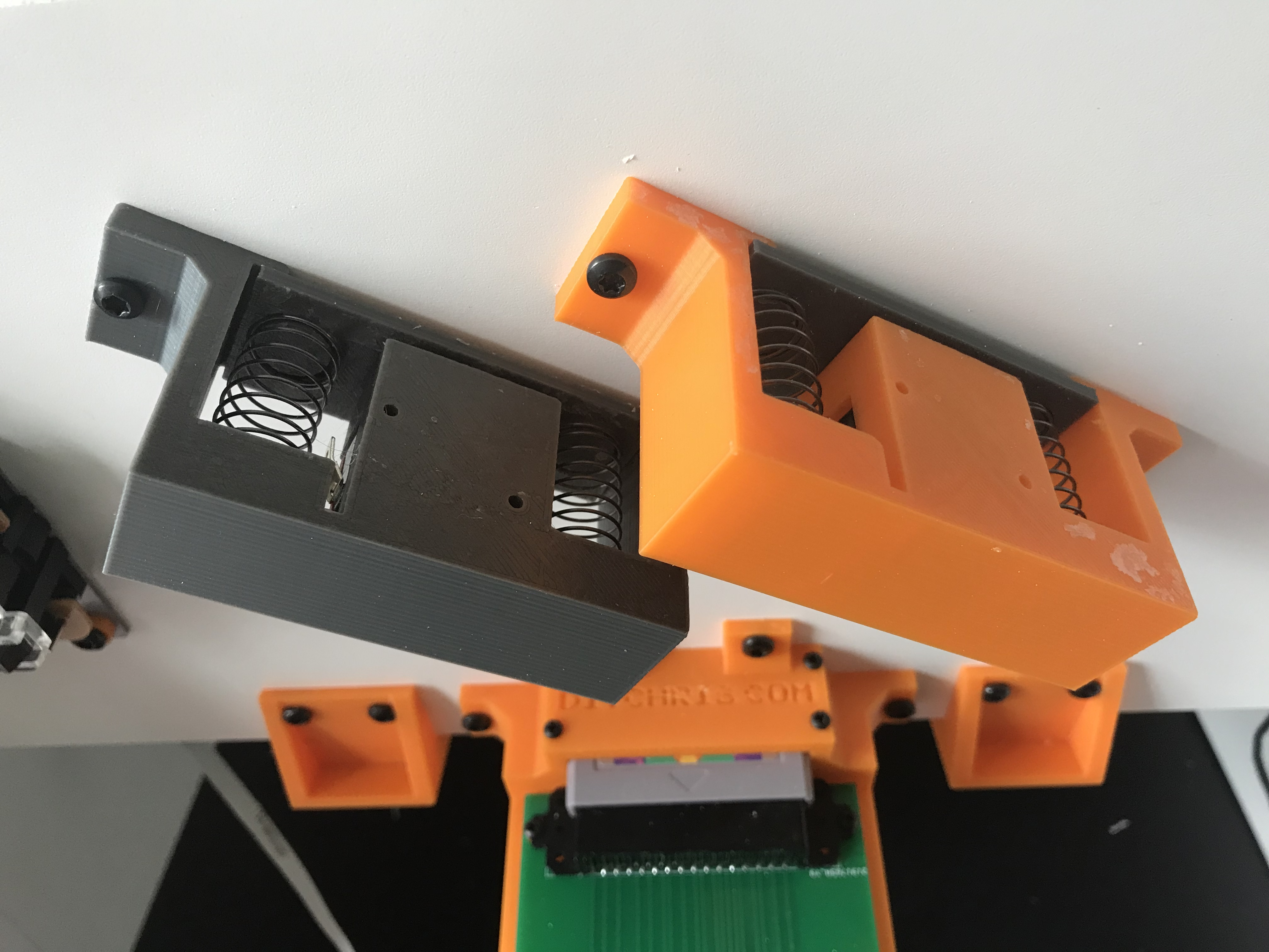
I’ve been working on this for a couple of months now and I am really liking how it’s coming along. The cabinet will be completely 3D printed and will be mostly press fit together with a few hidden brackets on the inside to keep everything tightly together.
My plan is to finish this project up in the next week or so and then offer DIY kits which will consist of all the 3D printed parts, the mainboard, LCD panel, and all the other little accessories you’ll need to build your very own ArcadeBoy. The only thing you’ll need aside from the DIY Kit to have a complete build is an original Gameboy. Everything is designed so that you can integrate your Gameboy in a non-destructive way. All that’s required is to remove all the screws, remove the top of the case and disconnect the screen.
Stay tuned for some pictures. I’m waiting on a few parts to be able to button it up and get it ready for its first photo shoot. As soon as I do, I’ll post pictures here for you all to take a look!
Update – 2019.08.17
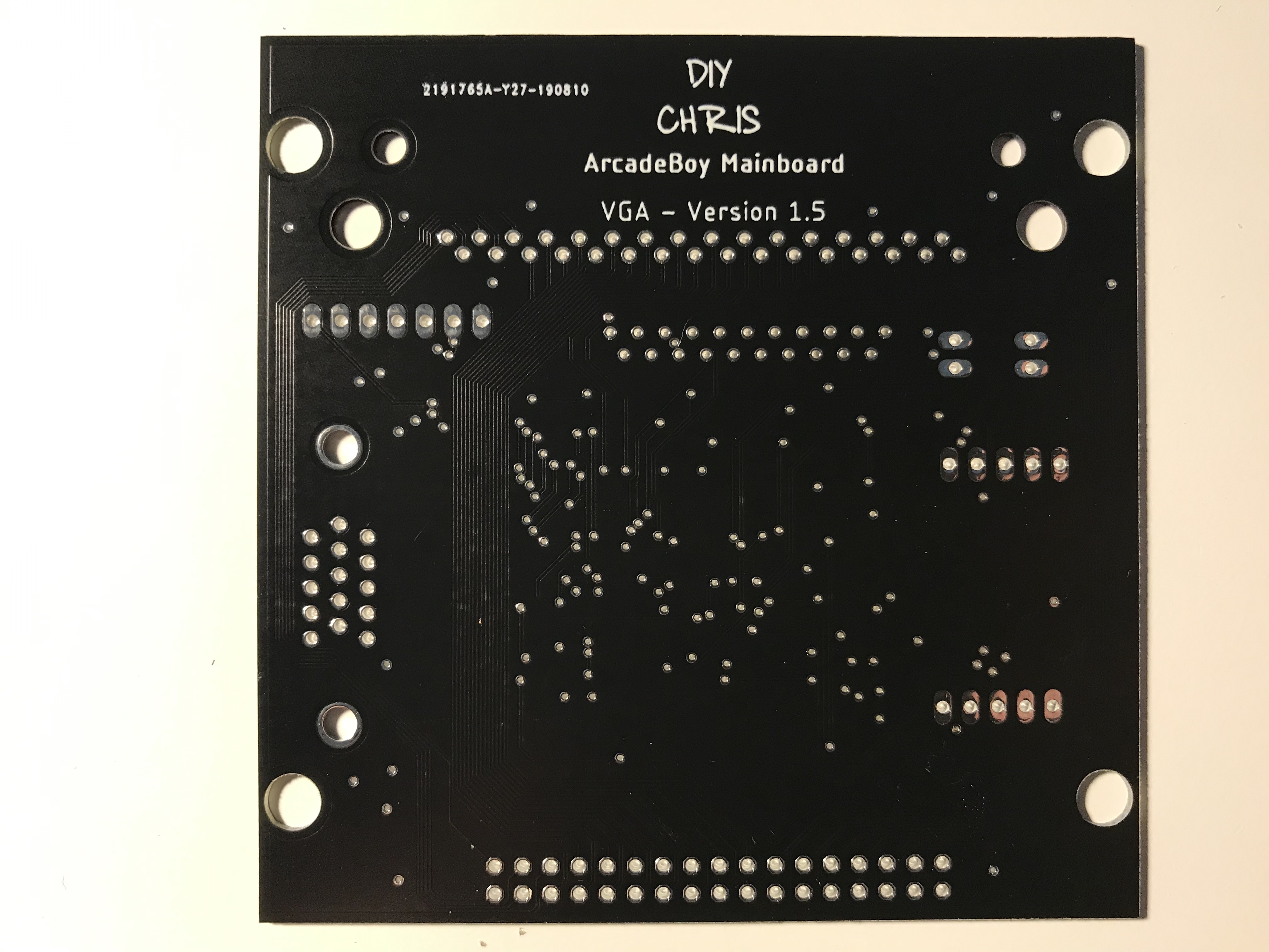
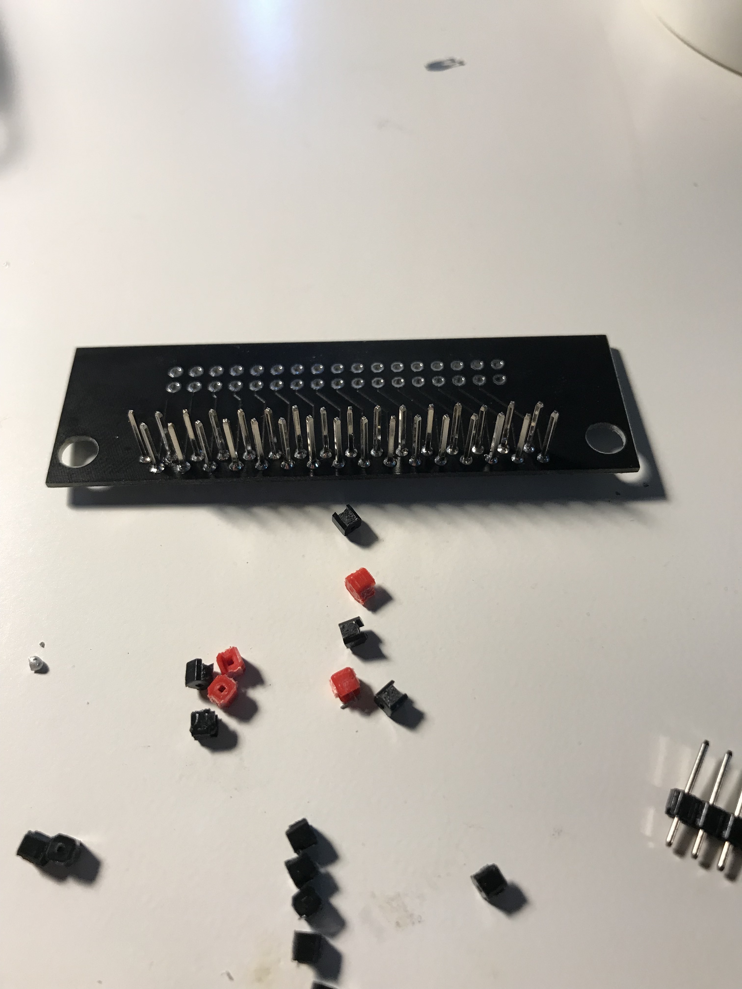
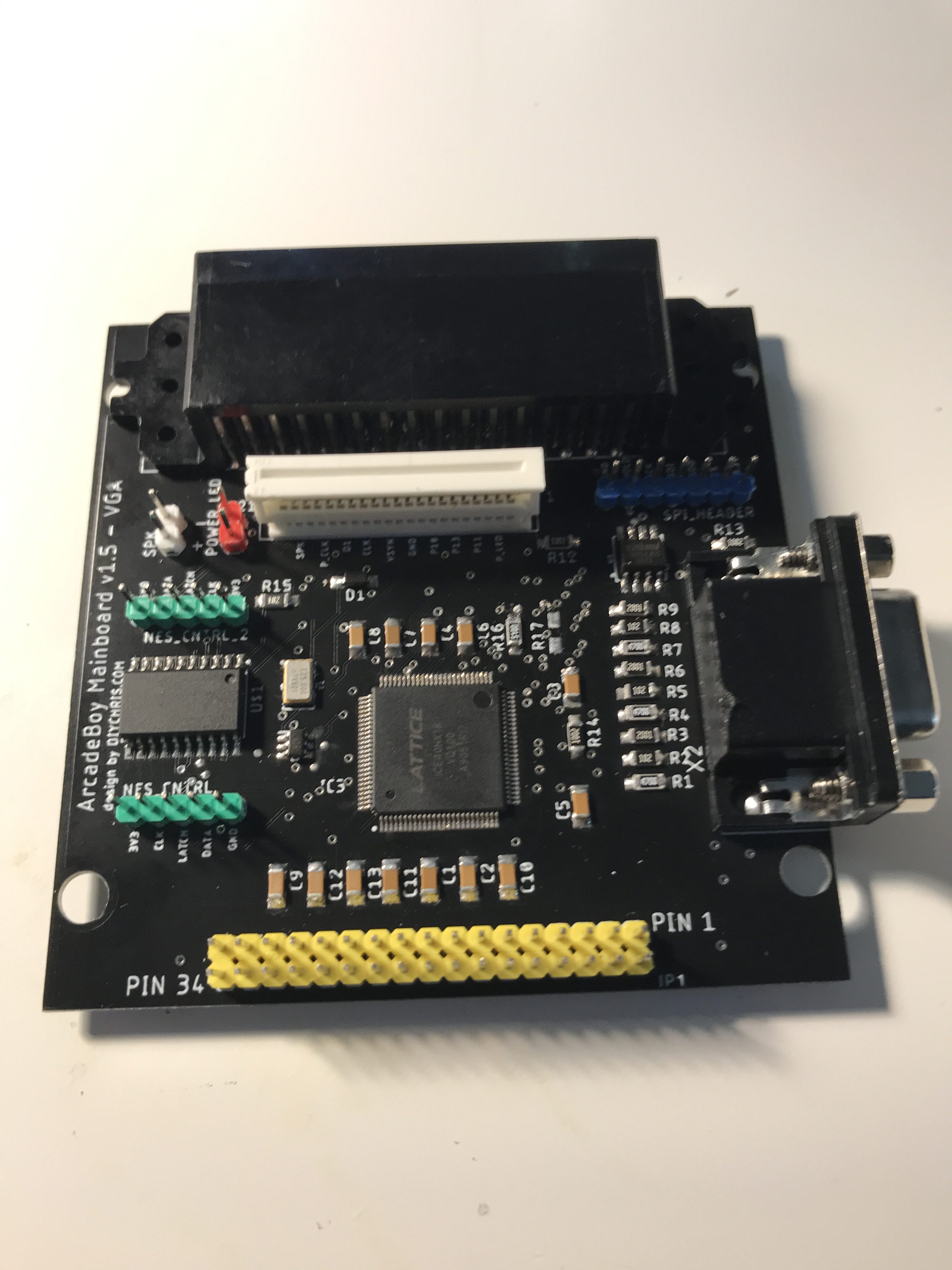
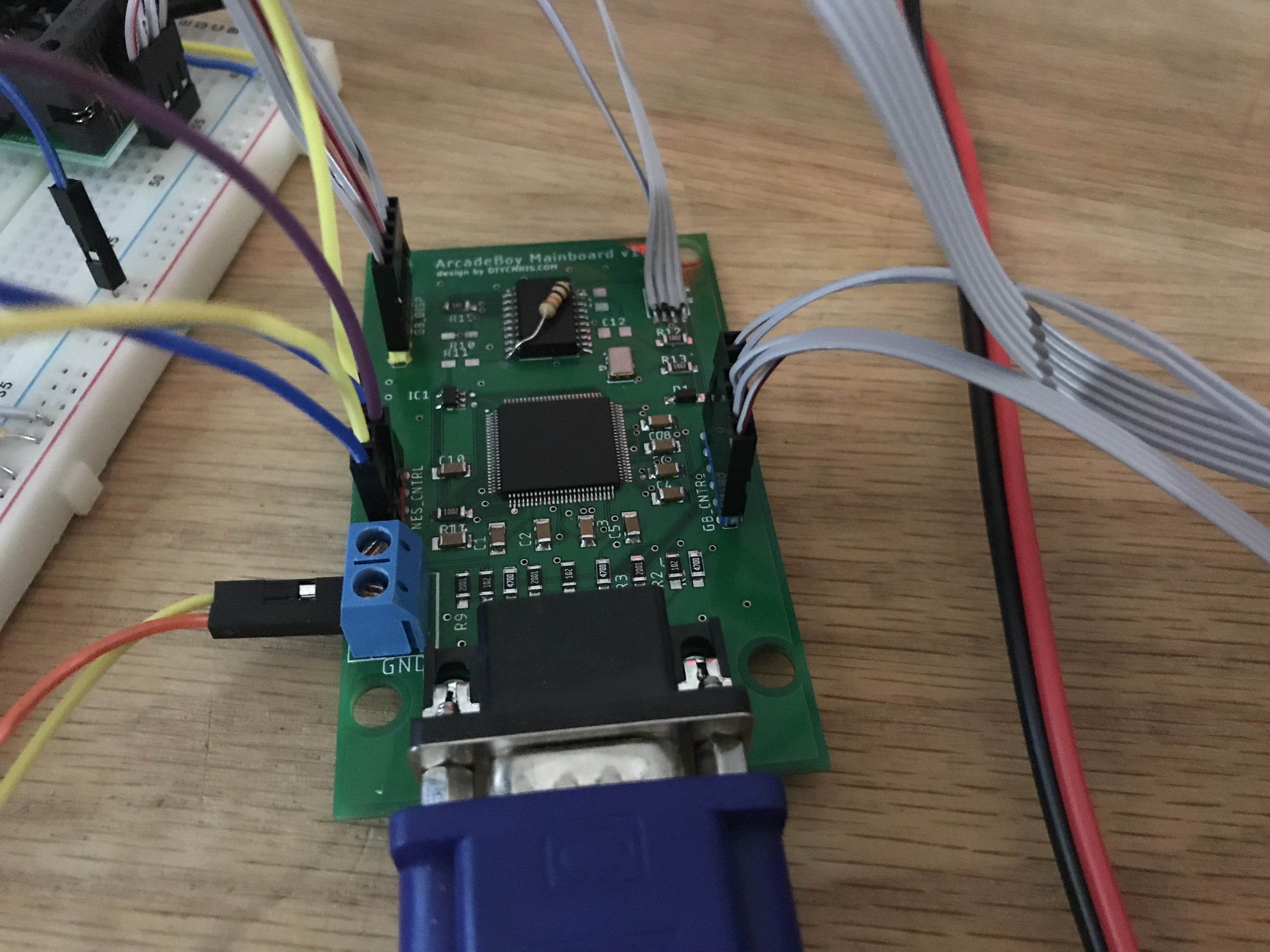
Big update this time. I received PCB’s from China on Thursday. Specifically, the ArcadeBoy Mainboard v1.5 which replaces the 2 voltage regulators 3.3v and 1.2v with one regulator that outputs 1.2 and 3.3 volts. I’ve also added headers breaking out the Speaker and Power LED from the DMG-01’s mainboard. I also updated the firmware on the FPGA to add support for a second controller so that the game can be played either with the arcade controls or an NES controller. Another big change on this revision is the pin header to connect to the cartridge connector to the DMG’s mainboard. I decided to go with a standard pin header since 34 pin IDC connectors are plentiful and inexpensive. Below is a picture of the board unpopulated front and back:
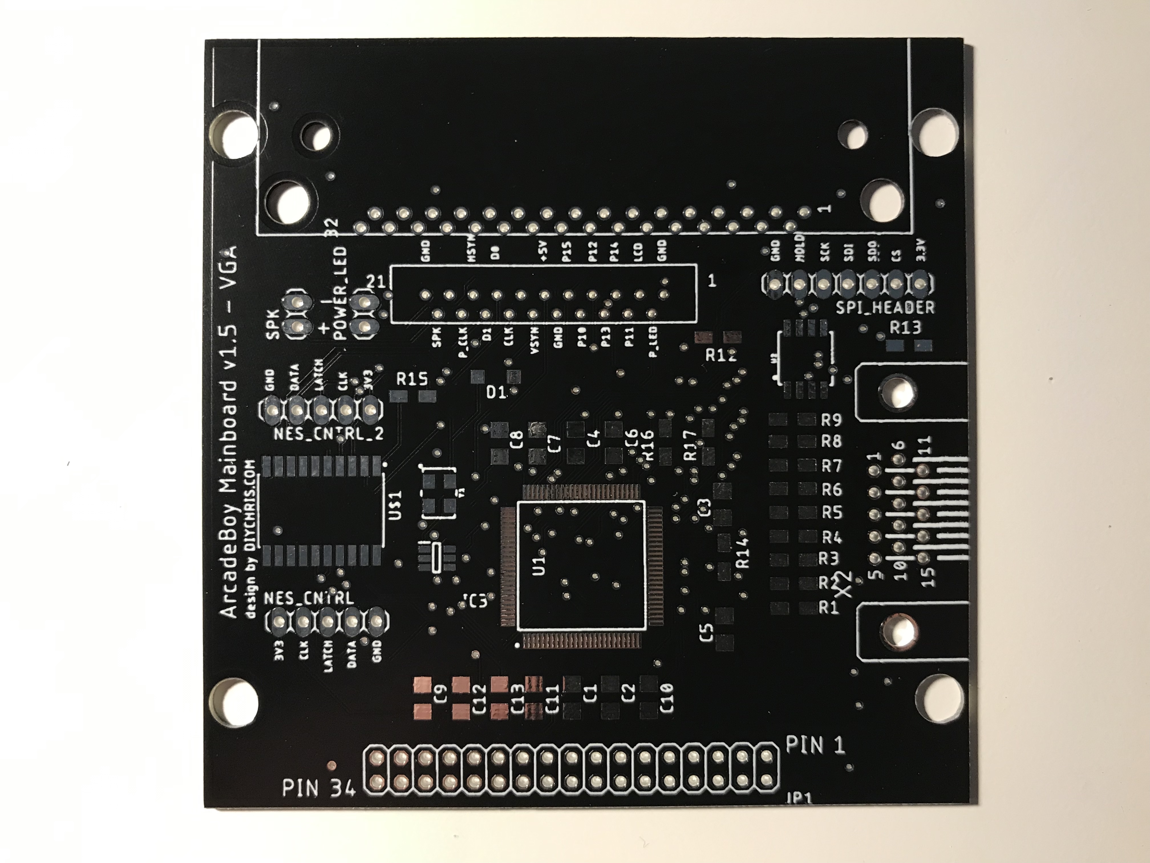
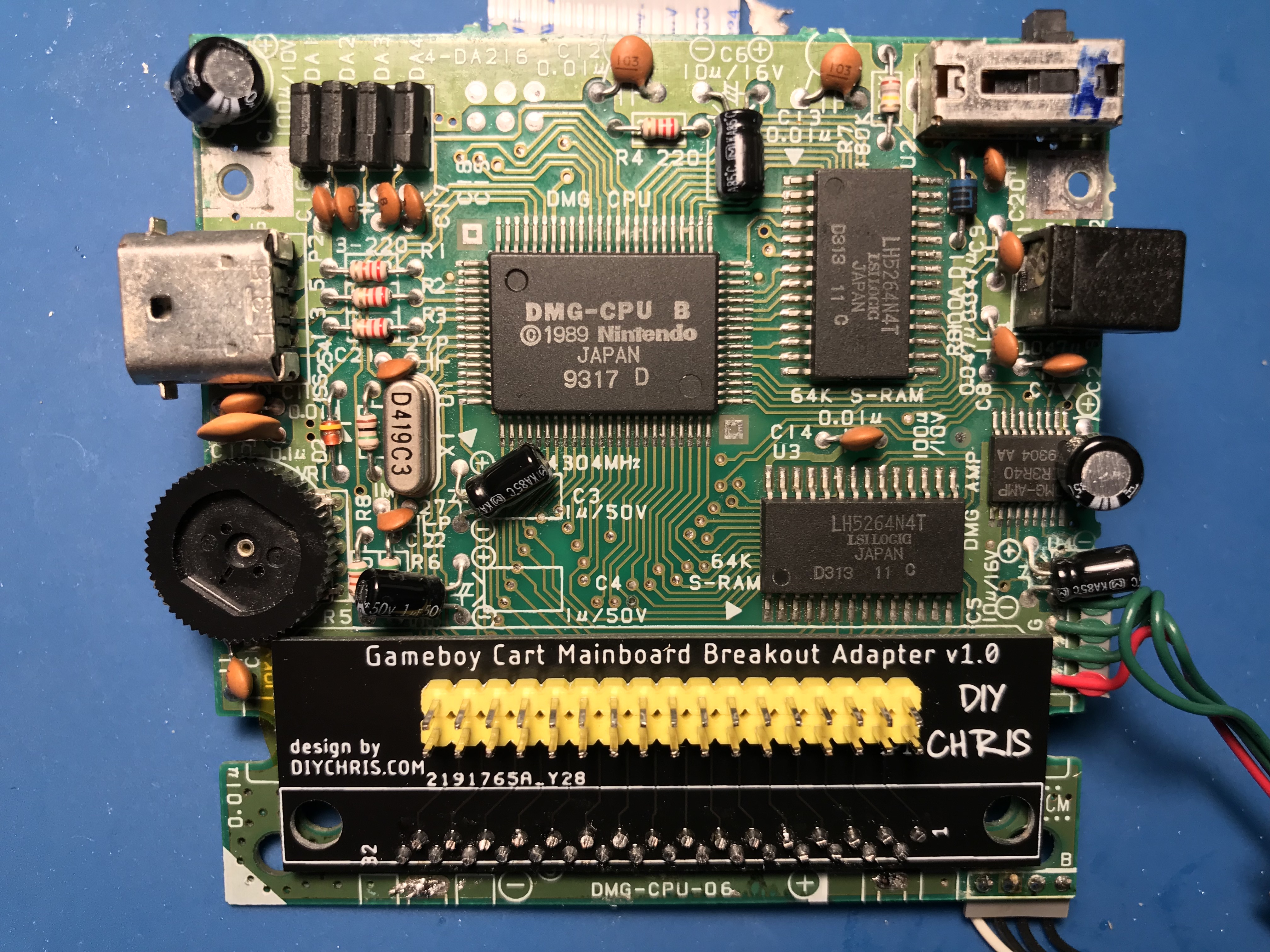
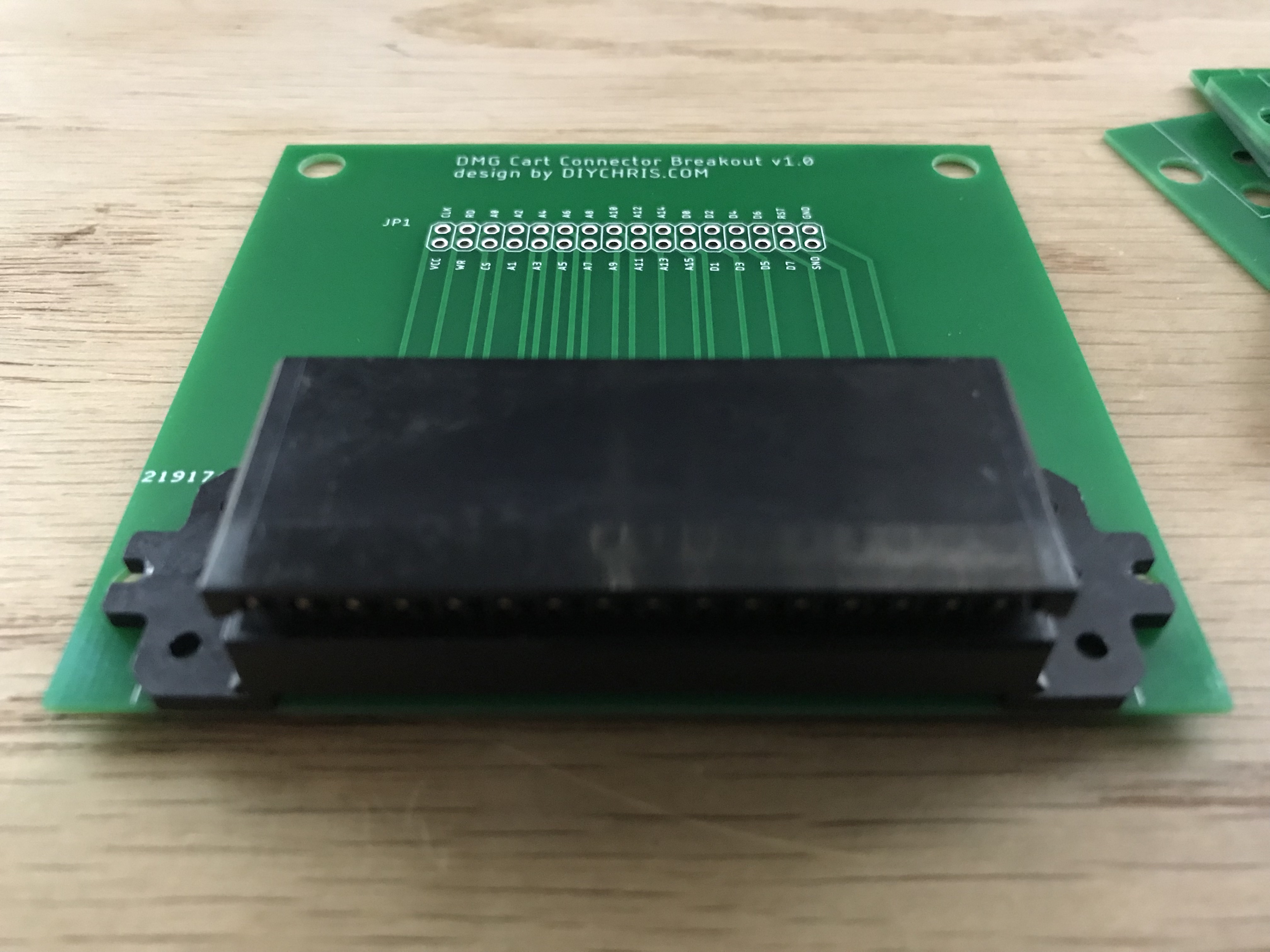
Since I decided to go with standard pin headers on the ArcadeBoy mainboard and I wanted a clean connection on the other end (the connection to the DMG-01 mainboard) I designed a breakout adapter that converts the DMG-01 mainboard pin header to a straight 34 pin connector.
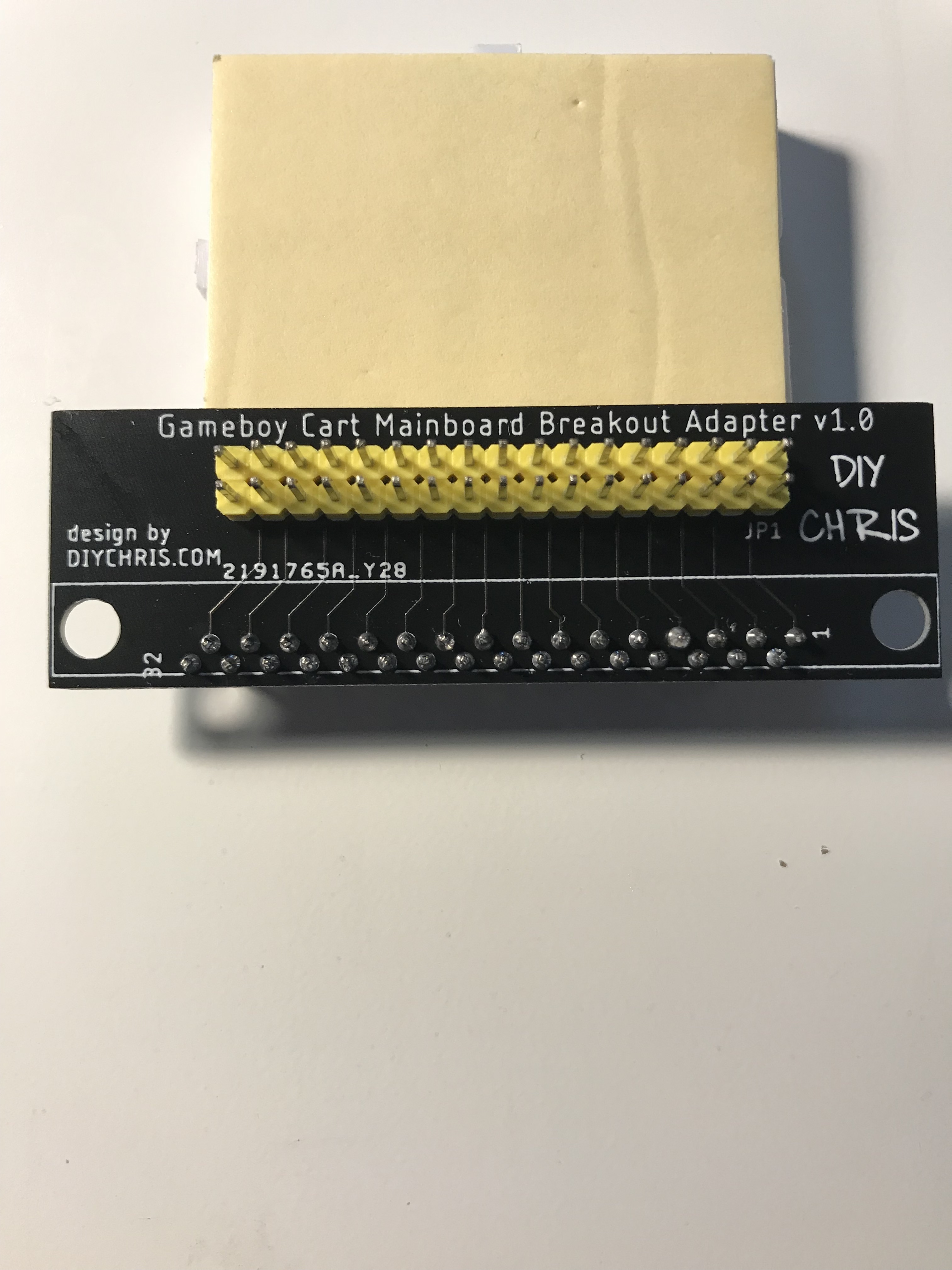
So the next step was to desolder the cartridge connector from the DMG-01 mainboard and then solder on my breakout adapter.
Anxious to get started, my next step was to start adding components to the ArcadeBoy mainboard, probably my favorite part of doing this. There’s something extremely therapeutic about soldering small surface mount components, especially when they’re being soldered to a super sexy matte black PCB.
So I managed to fry another DMG-01 mainboard. I guess I should have learned by now that the high voltage LCD pin being right next to the P11 pin which is responsible for left and B means that I need to make sure that there is no power applied to the board before removing or inserting the ribbon cable. I’m guessing that a fried that input pin on the CPU since there doesn’t seem to be a fuse or anything between that pin on the ribbon header and the pin on the CPU.
Ok, so I ordered a few more Gameboys on eBay just so that I have some spare boards to work with in case I make any more bonehead mistakes.
For now we will continue on with the board with the bad P11 pin since we can still do pretty much everything else we need.

If you look closely at the pictures above you’ll notice that I added some vinyl to the arcade controls. That was my first attempt at designing and having vinyl printed. Trying to get it to line up was an absolute disaster and there’s no way that I’m going to be using vinyl to finish this project. I’ve got a few other ideas such as latex paint which someone recommended. I decided to test how well the latex paint would stick to the PVC and it seems to hold up extremely well. I started with a base coat of plastic primer and then used a roller and some Lowes brand house paint mixed to try and emulate the color of the original gameboy. The paint I used went on well but even after about 3 weeks still feels a little tacky to the touch. I’m going to try a different brand of paint and will most likely spray it on instead of rolling it on because I didn’t really like the texture it left behind.
So what’s next?
I need to finish designing the rest of the cabinet and work out how I want to handle the sound. I also need to design a button that can be used to turn the ArcadeBoy on and off similarly to how the Gameboy on/off button functions.
Stay tuned for future updates.
Update – 2019.08.13
Not much of an update from the last one other than the revisions of PCB’s. I’m actually up to version 1.5 now, with 1.5 being the one currently on its way from China and 1.4 being the one from the pictures below:
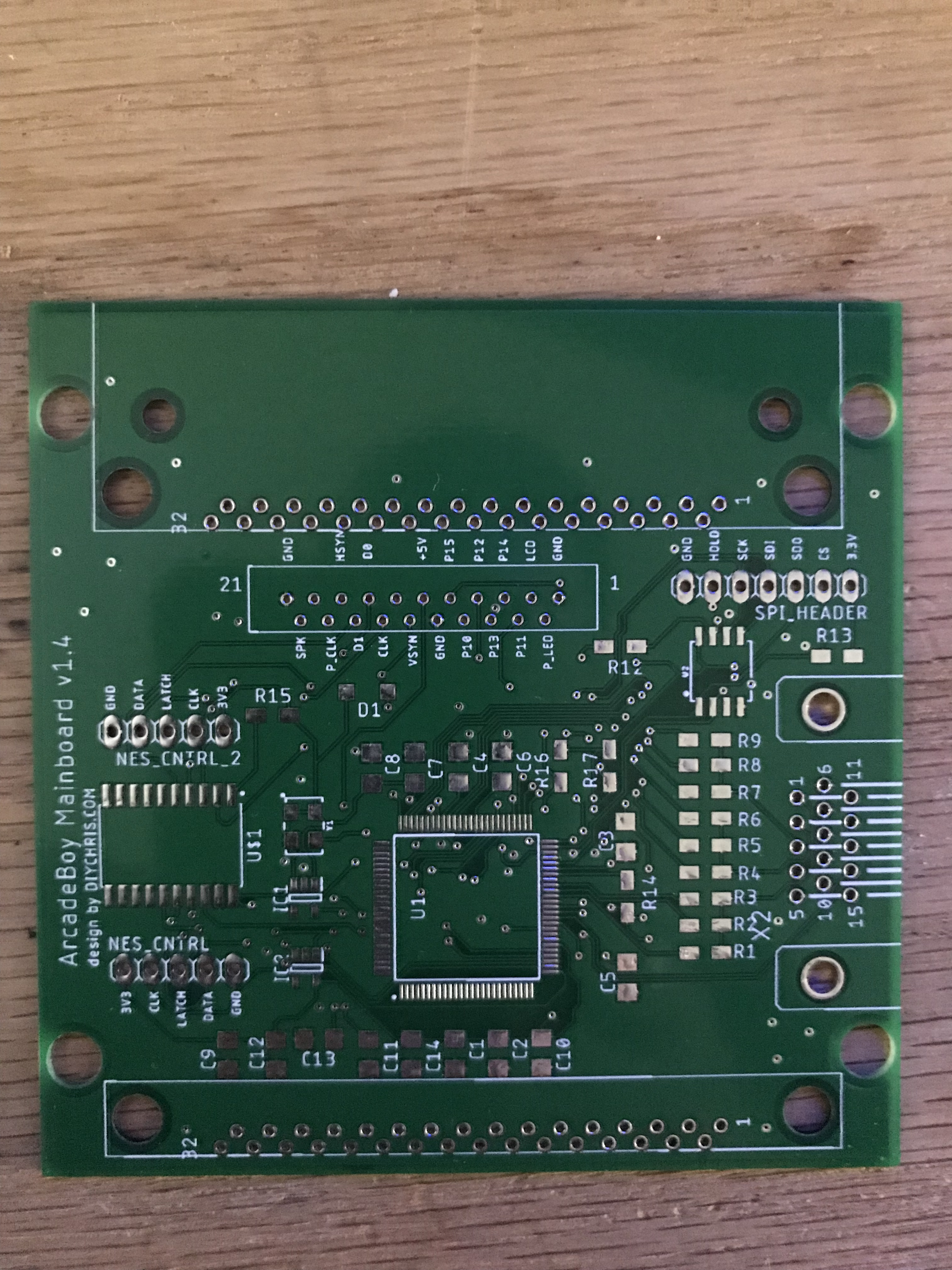
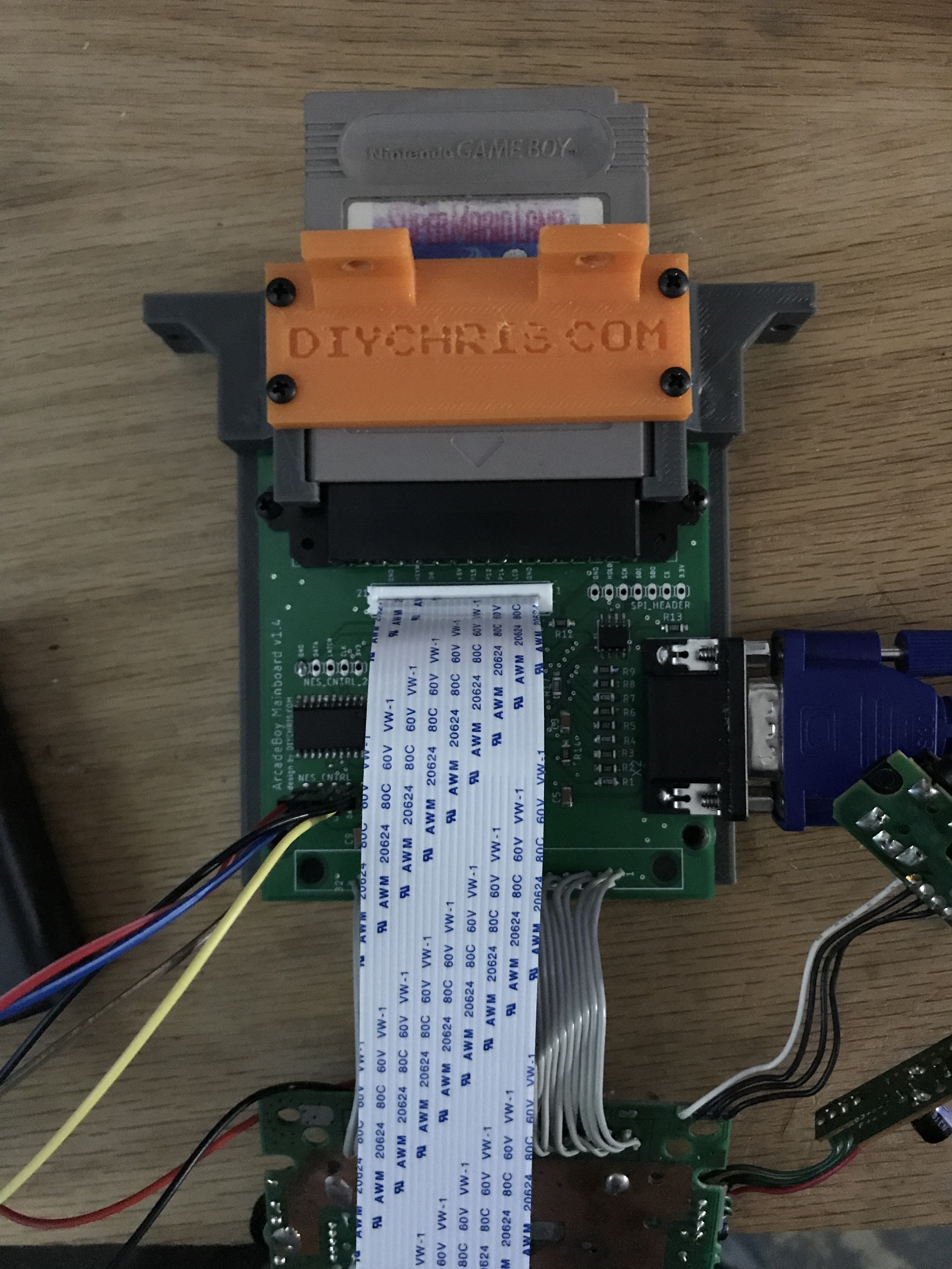
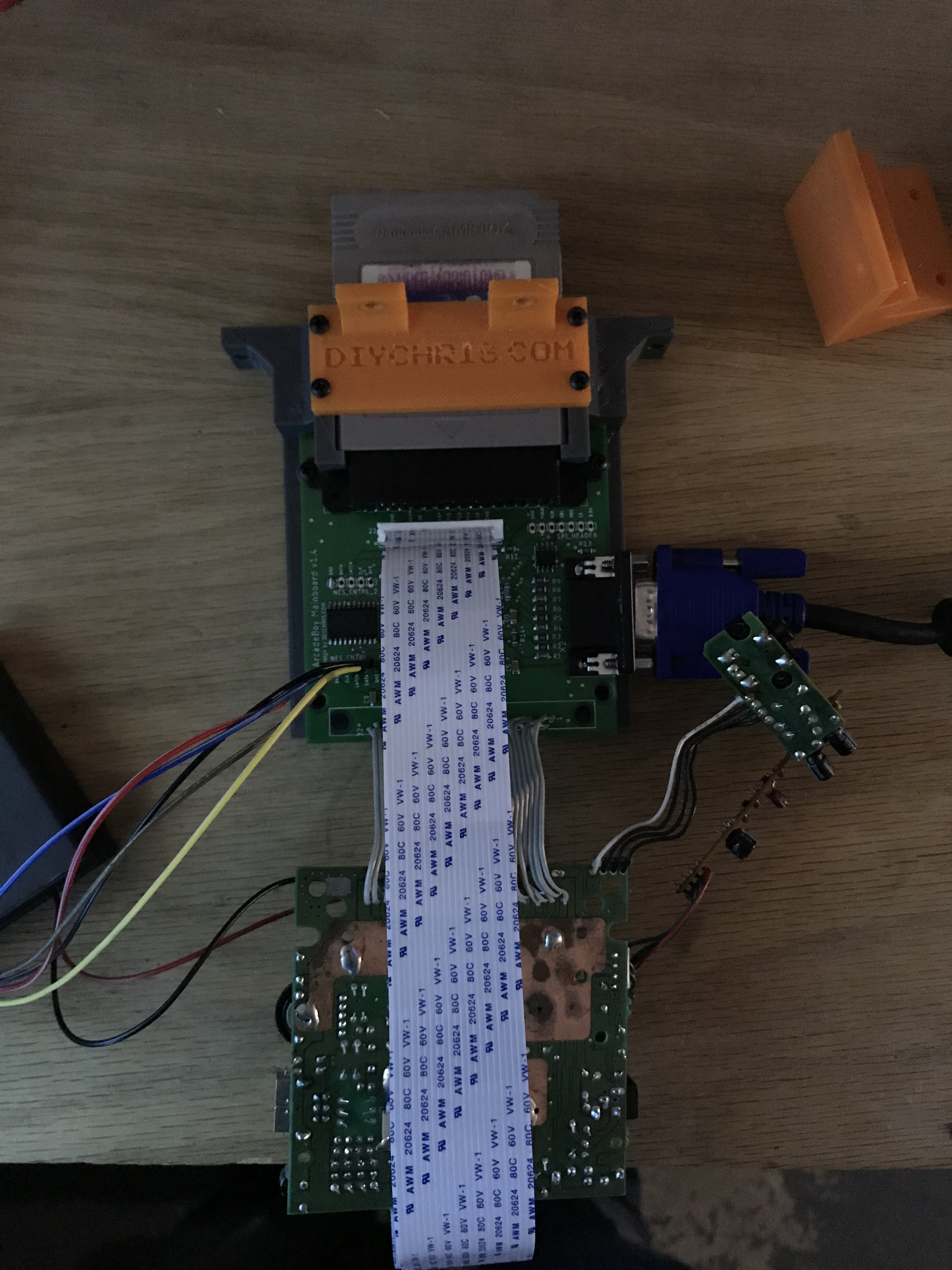
If you look at the pictures above you’ll see that I’ve integrated everything onto the PC board. I’ve gone as far as adding a 21 pin connector to connect to the DMG’s mainboard directly with a ribbon cable. The cartridge connector needed to be moved from where it was originally on the DMG mainboard so that it can accommodate how I want the cartridge mechanism to interface with the Arcade.
Its all working now and I’ve designed a “final revision” of the PCB, hopefully.. Of course, the ultimate plan is to move away from VGA and utilize HDMI which is something I’ve already been working on but is not my primary focus since I really want to get this done and start focusing on the structure and details of the Arcade.
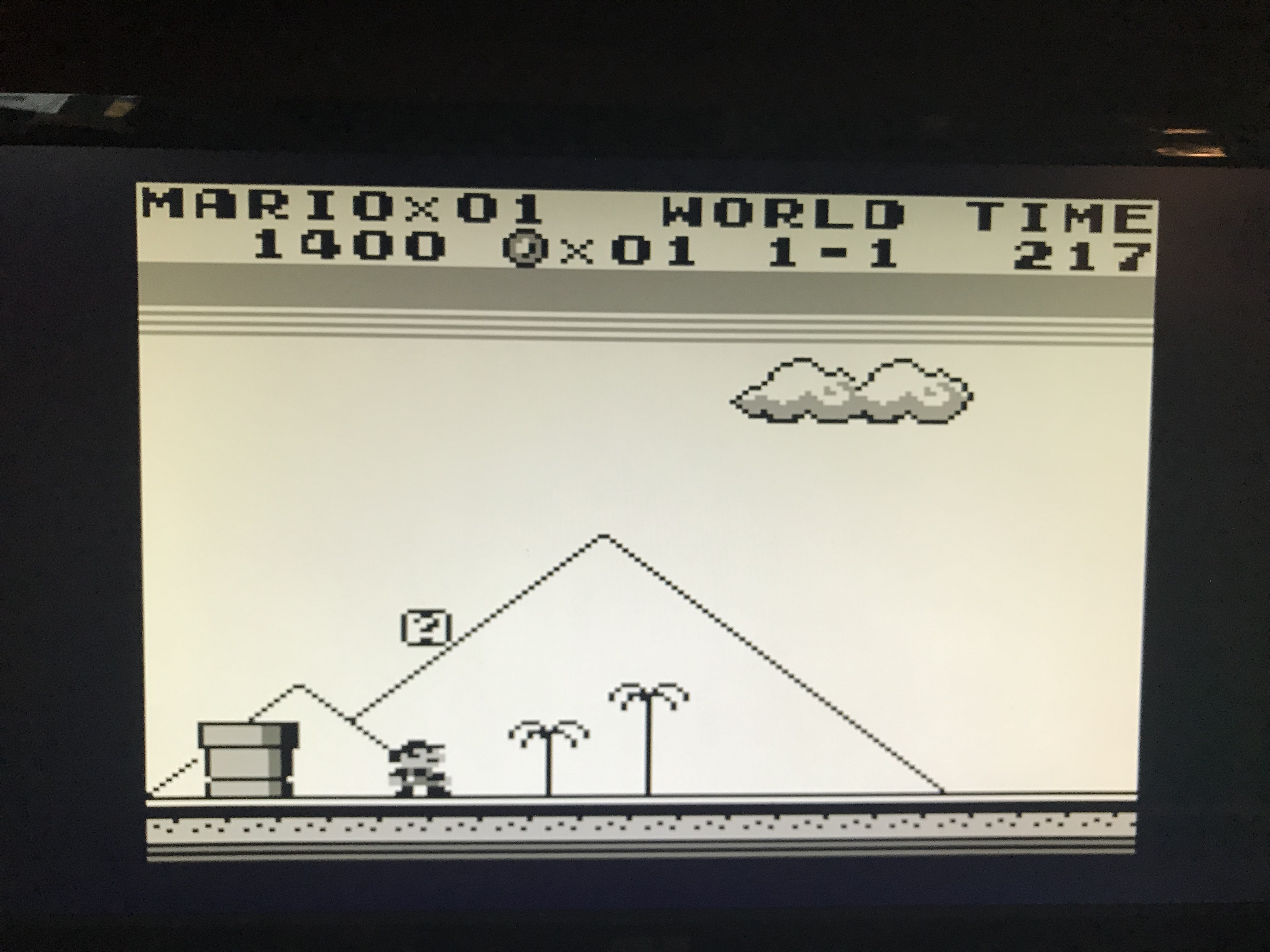
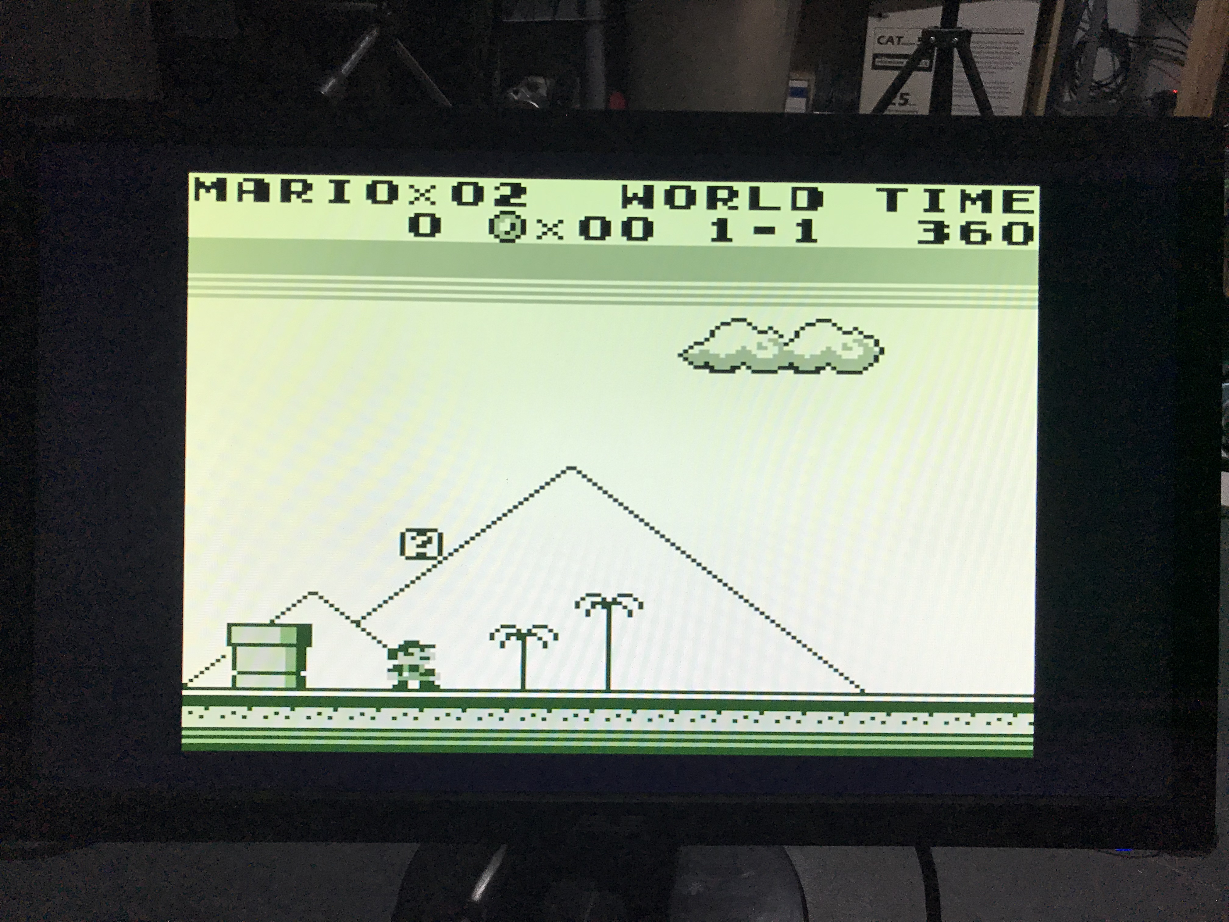
For now this is all I have for updates. Should have more this weekend. Hoping to be playing Super Mario Land on the Arcade!!!
Update – 2019.07.28
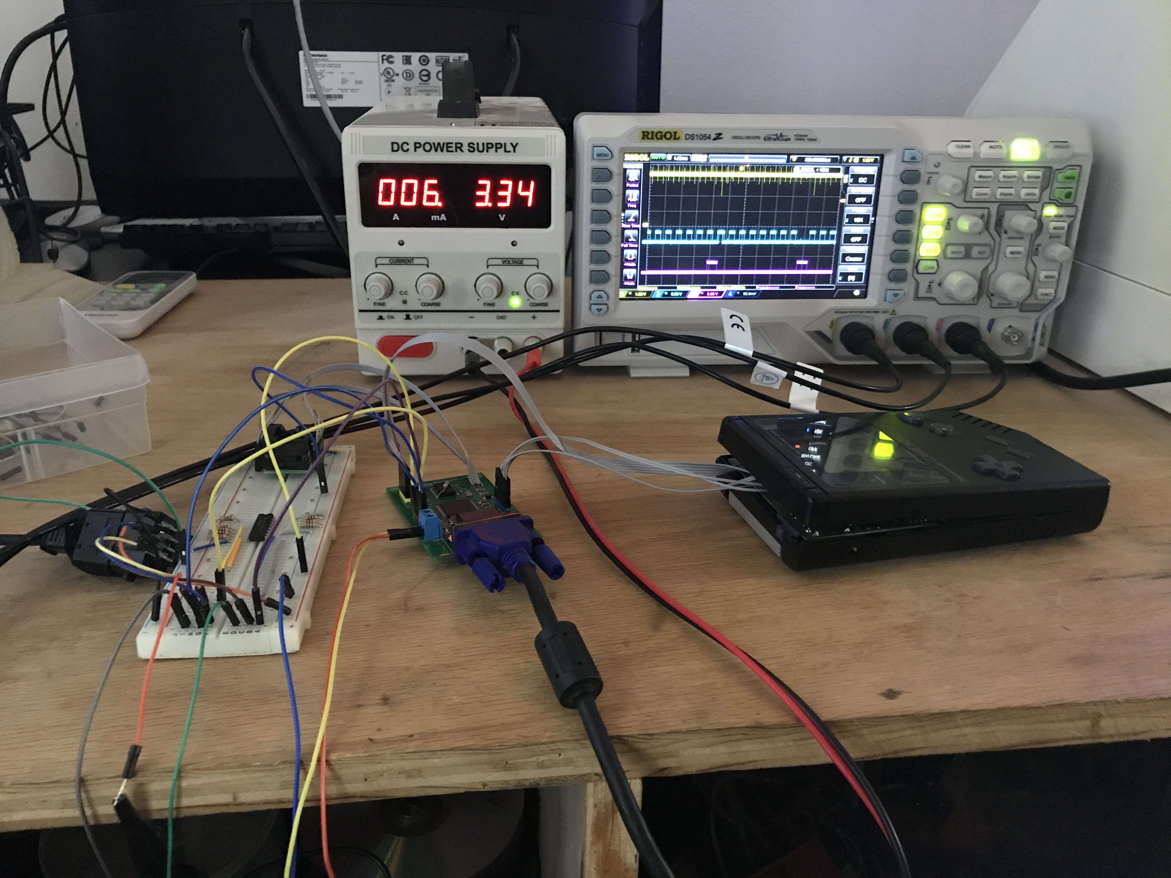
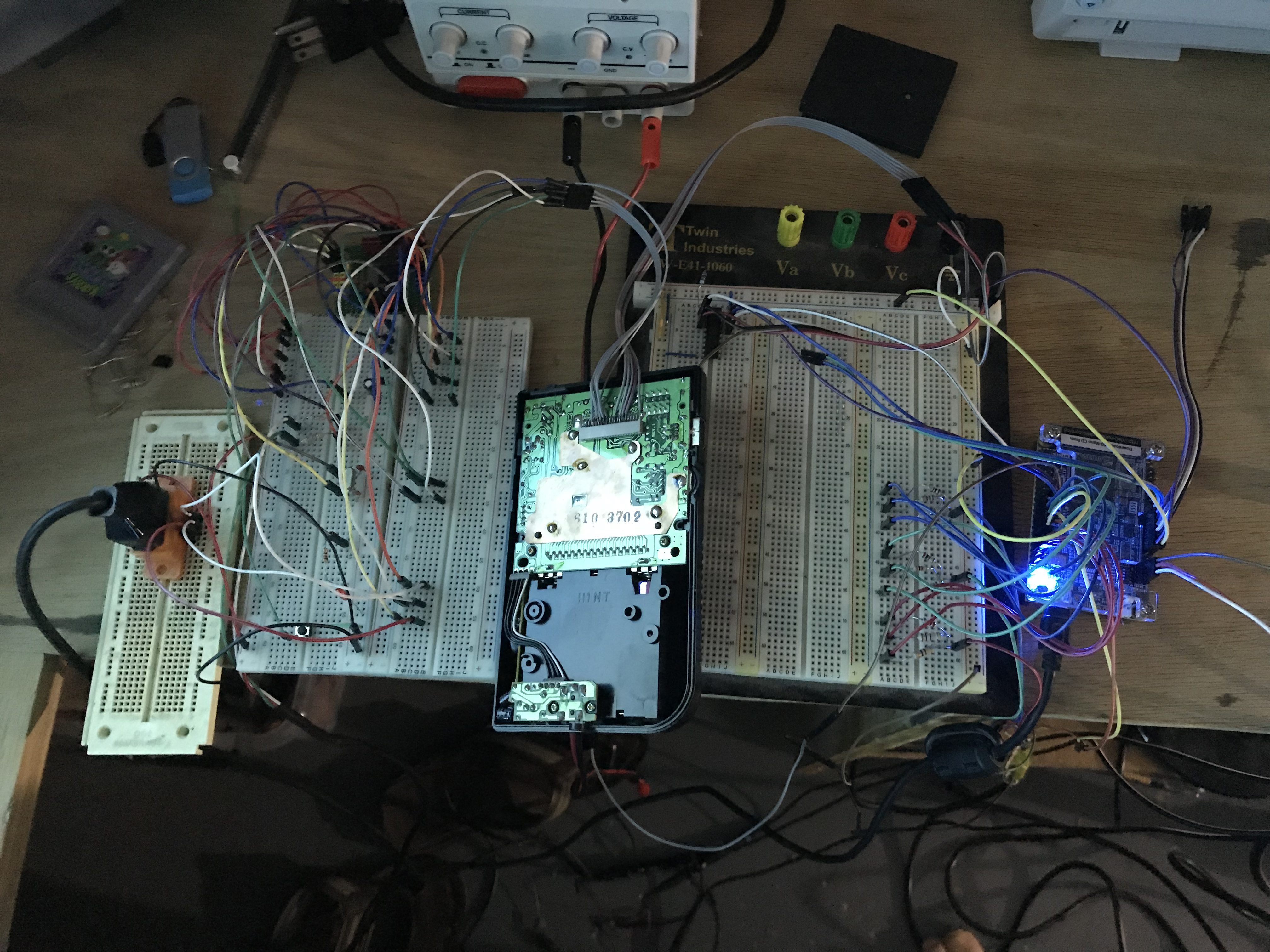
So I received the PCB’s from China last Monday. Of course the first thing I did was populate all the components starting with the 100 pin FPGA, then all the other IC’s (level shifter, voltage regulator, flash memory) and then moving on to the resistors and capacitors, finally finishing with the through hole components.

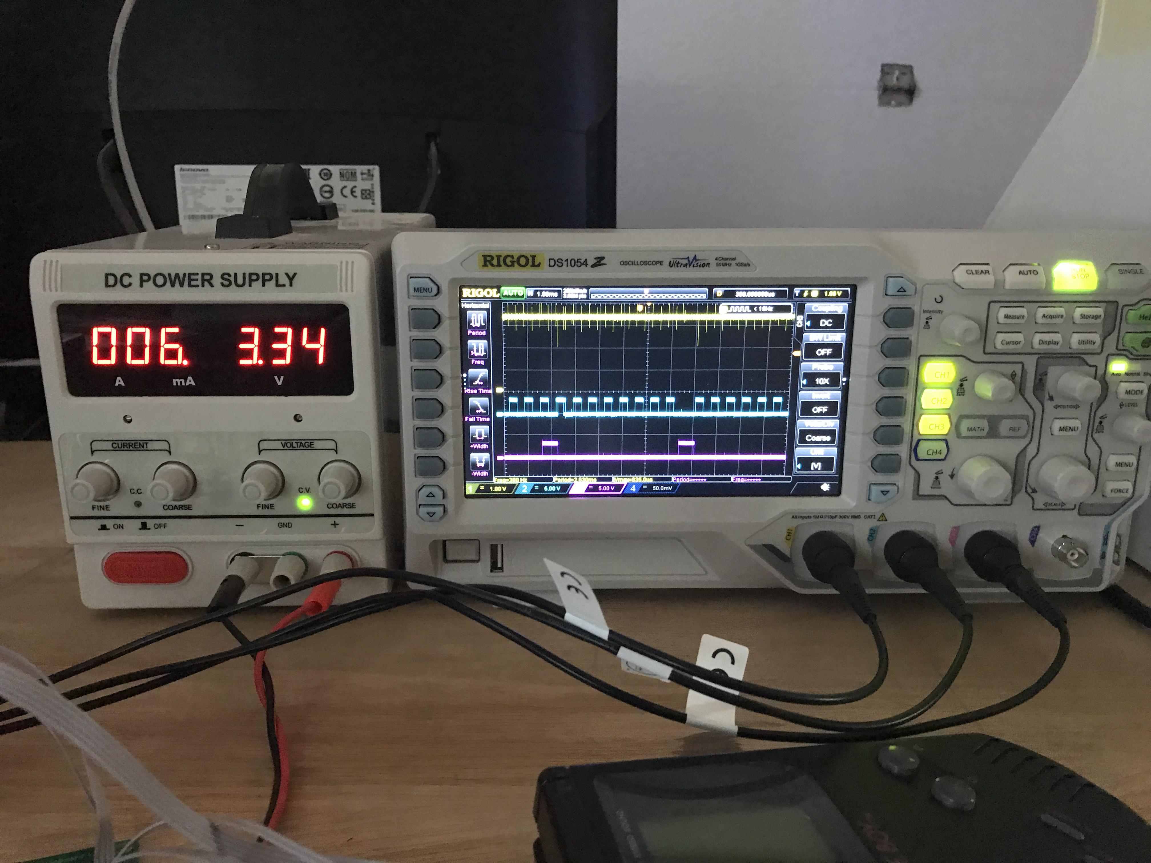
I inspected everything and checked for any shorts, all seemed well. I plugged in the gameboy mainboard the NES controller and the VGA monitor and applied power and… …nothing.. nothing at all. My monitor continued to display VGA no signal. Wonderful, so it was time for troubleshooting. Who was I to think that it was just magically going to work on the first try.
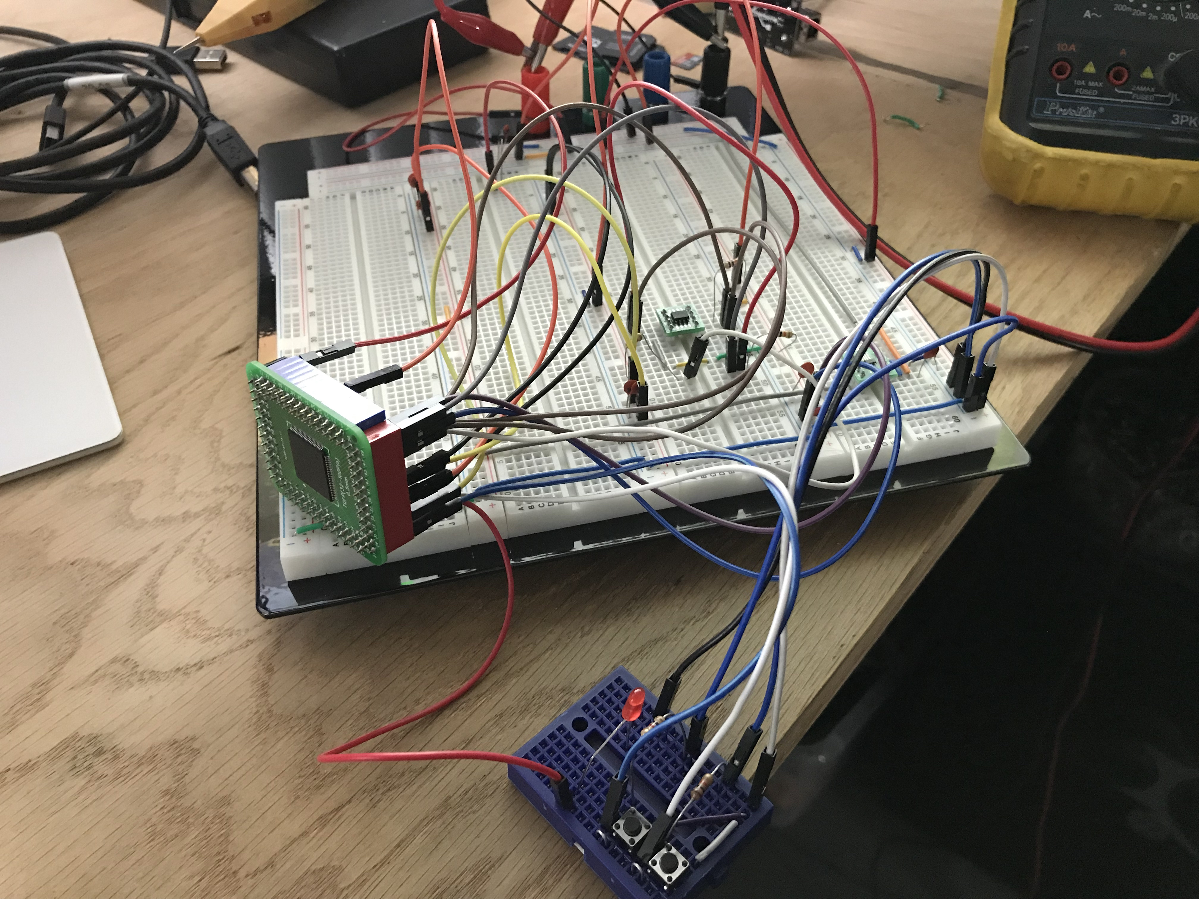
So after troubleshooting for a bit, I found my first mistake. I accidentally swapped the SDI and SDO connections on the flash memory so the FPGA wasn’t configuring itself. The indicator there was that the CDONE pin on the FPGA remained low. This pin goes high when the FPGA is configured. So I improvised by desoldering the flash memory and soldered on ribbon cables and attached those to a breadboard along with a SOIC-8 ZIF socket so I could easily reprogram if I had to.
Now I got the CDONE pin going high to I know the FPGA is configured. I was also now getting a VGA signal but I was not getting what was supposed to be on the gameboy. I just had a blank gray screen. So the first thing I checked for was if I was getting data, clock and sync signals from the gameboy at the input of the level shifter which I was, but I wasn’t getting anything on the output. Looking over the data sheet of the level shifter it specifies enabled as being active low which I thought meant that it was internally tied to low which apparently was not the case. I soldered a pull down resister between the /OE and GND pins of the level shifter and guess what… it works.
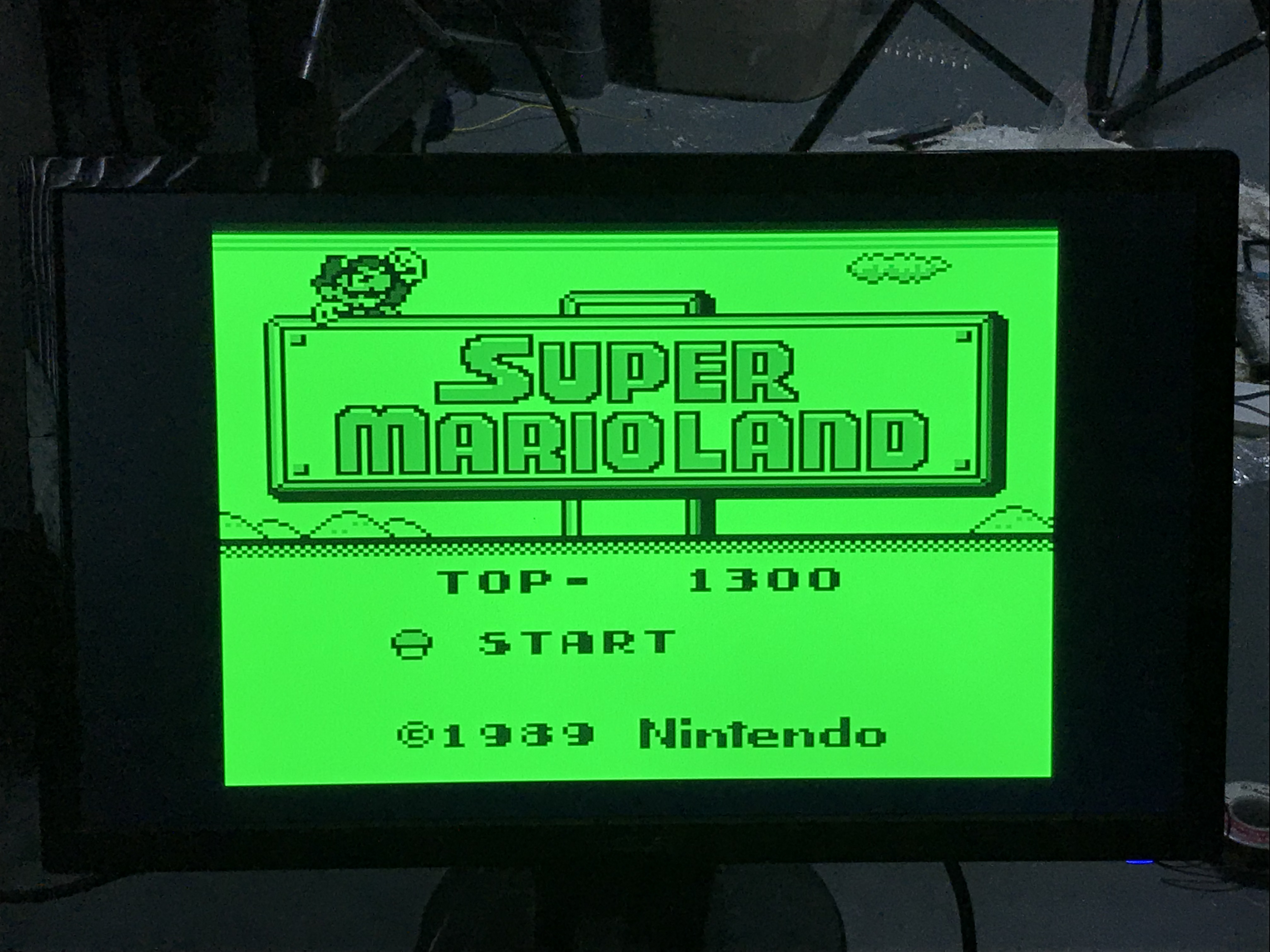
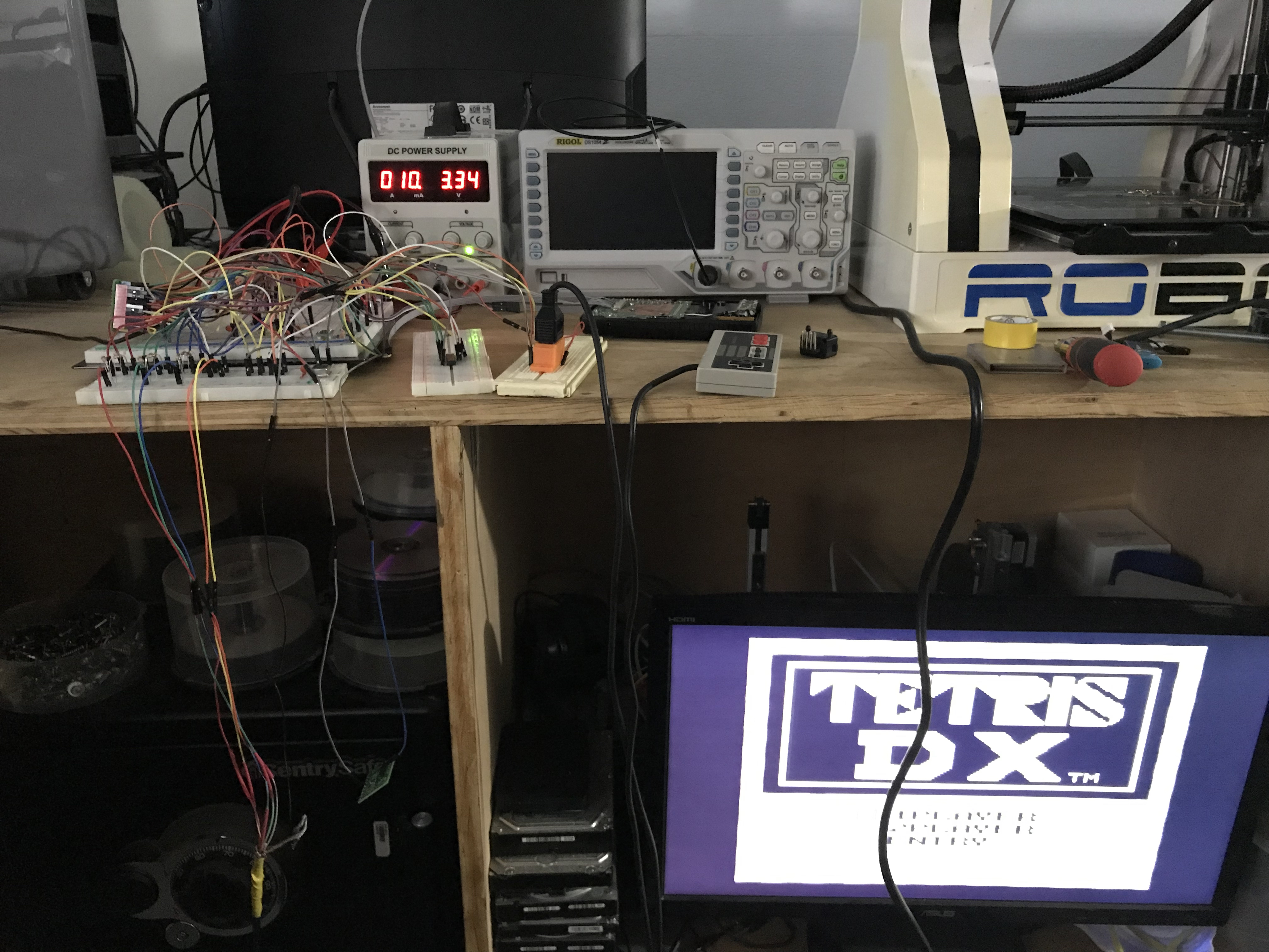
So now I have a nice sharp signal coming from the gameboy to my monitor. Check it out:
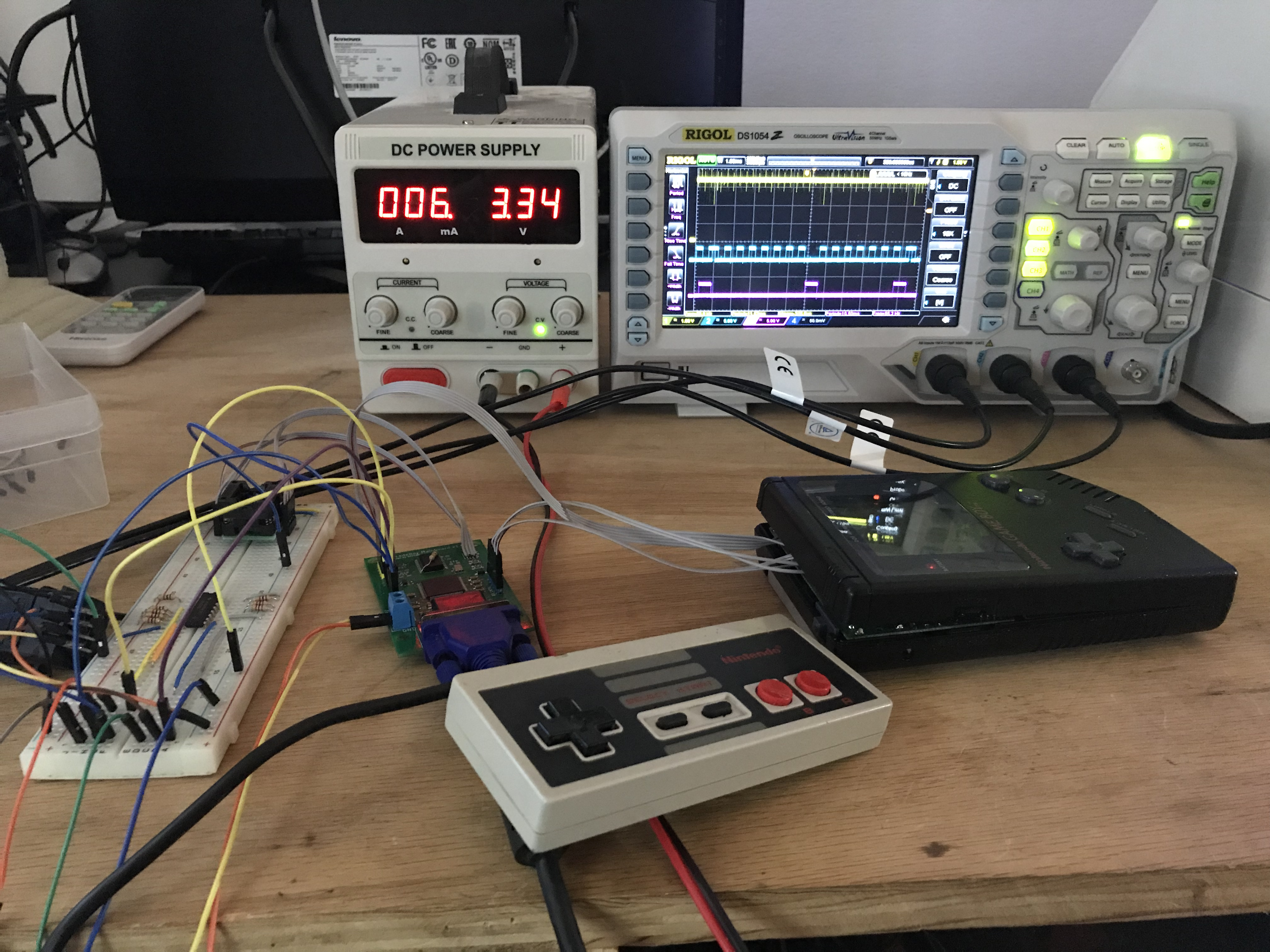
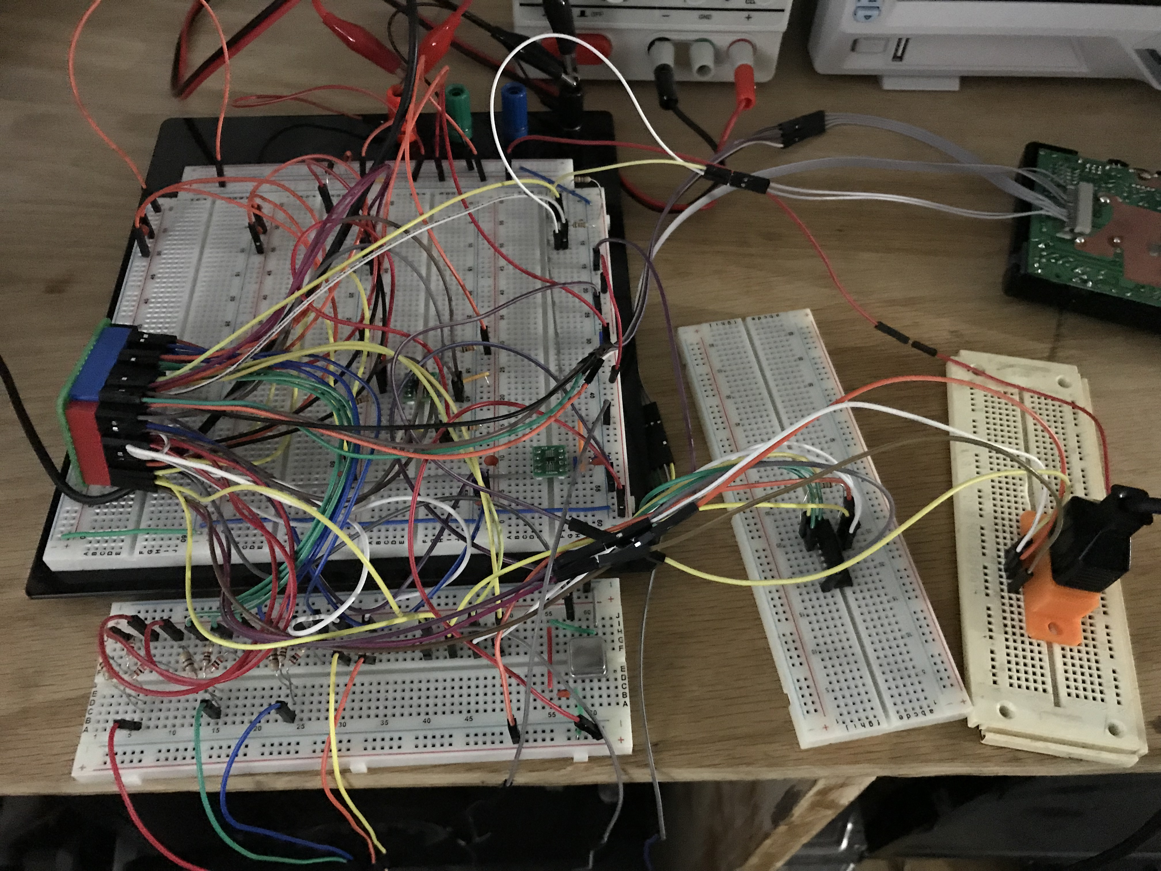
Onto the next problem, the controller. This thing was a pain in the ass even back when I was developing on the bread board but I figured that a lot of the issues where due to noise from all of the wires all over the place. Well it didn’t work. It must have taken me a few days to figure out what the problem was which is actually a bit embarrassing but these things happen. I apparently had a short on the data input pin on the ArcadeBoy’s mainboard which caused the data input to be held at around 1 volt which is way below registering as a high. The gameboy’s buttons are enabled active low so obviously it assumed that all buttons were being pressed. Unfortunately I couldn’t find the short so I started over on a new clean board, each time testing for shorts as I soldered on a group of components.
What I was left with was a working board.
What’s next? The next iteration will incorporate the fixes I had to improvise. I’ve also included an SPI header so that I could reprogram the flash memory if I needed to.
I should have the new board on Monday at which point I’ll be soldering all the components again. Hopefully this time I won’t run into so many issues. If everything works as expected, I’ll be working on my final revision which will incorporate the DMG cartridge connector and a ZIF connector to connect the mainboard effortlessly to the gameboy.
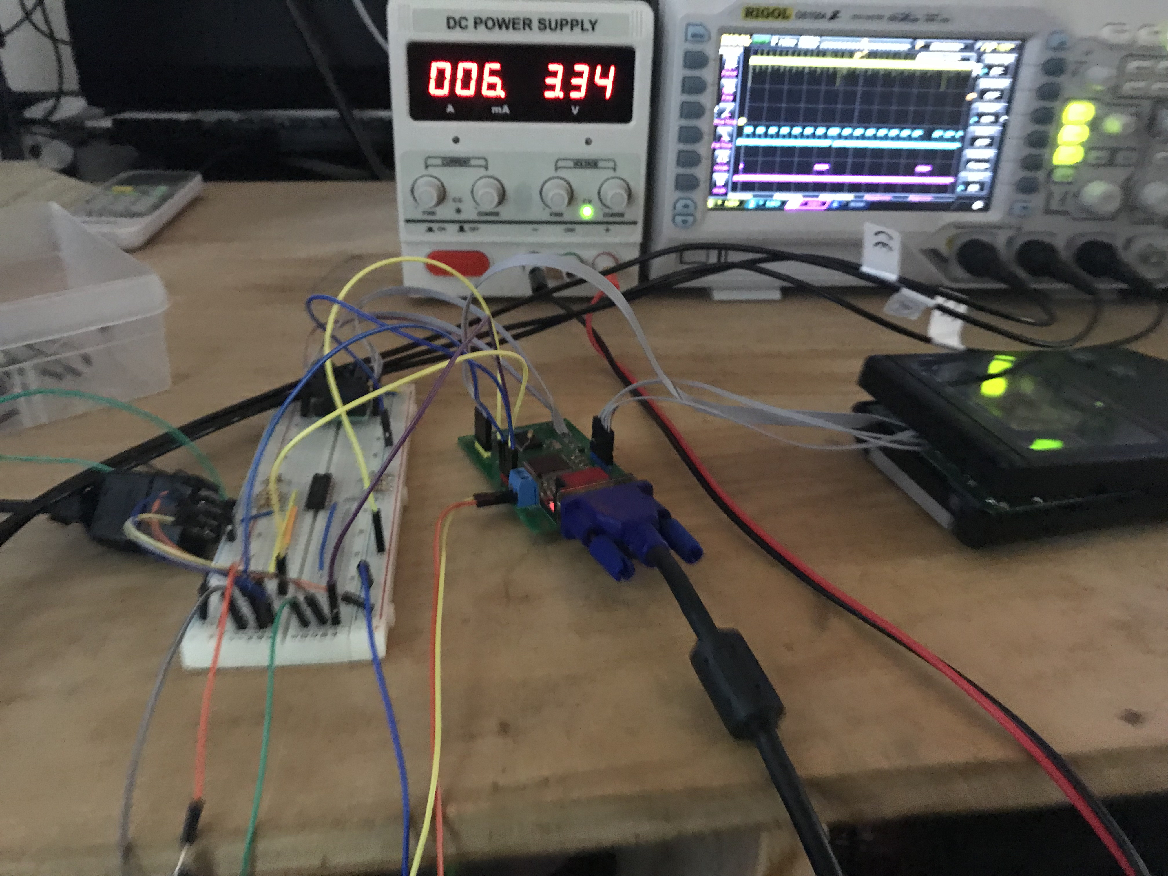
Here are some more pictures of the end result:
Oh, almost forgot, here’s a video of the progress. Probably much more fun to look at then the pictures, enjoy!
[embedyt] https://www.youtube.com/watch?v=c-MbWaHp2Kc[/embedyt]
First Entry – 2019.07.21
For some time now I’ve been wanting to mod my original Gameboy to provide VGA out so I can play on a big screen. I could just use the Super Game Boy for the SNES but it somehow doesn’t feel right to me. It feels like I’m cheating somehow. So I started looking around and it seems there are a few products out there that allow you to easily mod a Gameboy for VGA output but why use someone else’s product when I can make my own? This happened to be just around the time I started getting into FPGA’s and I felt like this would be the perfect project to undertake to build experience with FPGA’s and Verilog in particular.
I had a DE0-Nano back from when I took a digital electronics class in college that’s been sitting on a shelf collecting dust. I decided to fire it up and dig up some of my old school projects. Back then they were teaching us VHDL and at the time I actually preferred it over Verilog but the more I started using Verilog the more I started hating VHDL. So long story short, I found an online community where a guy built a VGA out using an FPGA for an Arduboy which coincidentally with a few modifications also worked well for a Gameboy. This is where my journey really began. Once I got the FPGA taking input from the Gameboy and outputting to VGA, I wanted to do more.
I’ve recently gotten into the hobby of designing and building table top (mini and medium sized) arcade machines running on a mix of PC and Raspberry Pi devices. I thought, how cool would it be to build an arcade machine around the Gameboy hardware? The answer? SUPER COOL …and this is where my project begins on the journey to build ArcadeBoy
Here are a few pictures of the progress so far:
I thought about how cool it would be to play old Gameboy games on original Gameboy hardware but in an arcade style fashion and realized that it would be a whole lot of fun if I could somehow incorporate an NES controller into ArcadeBoy so that if I wanted to, I could just plug in an NES controller and use that to play with.
The task was not a simple one. I actually had a lot of help from one UxE over at the Arduboy community forums to help out with this bit of the process. Eventually with his help, we got it working beautifully. Here’s a picture of the mess:
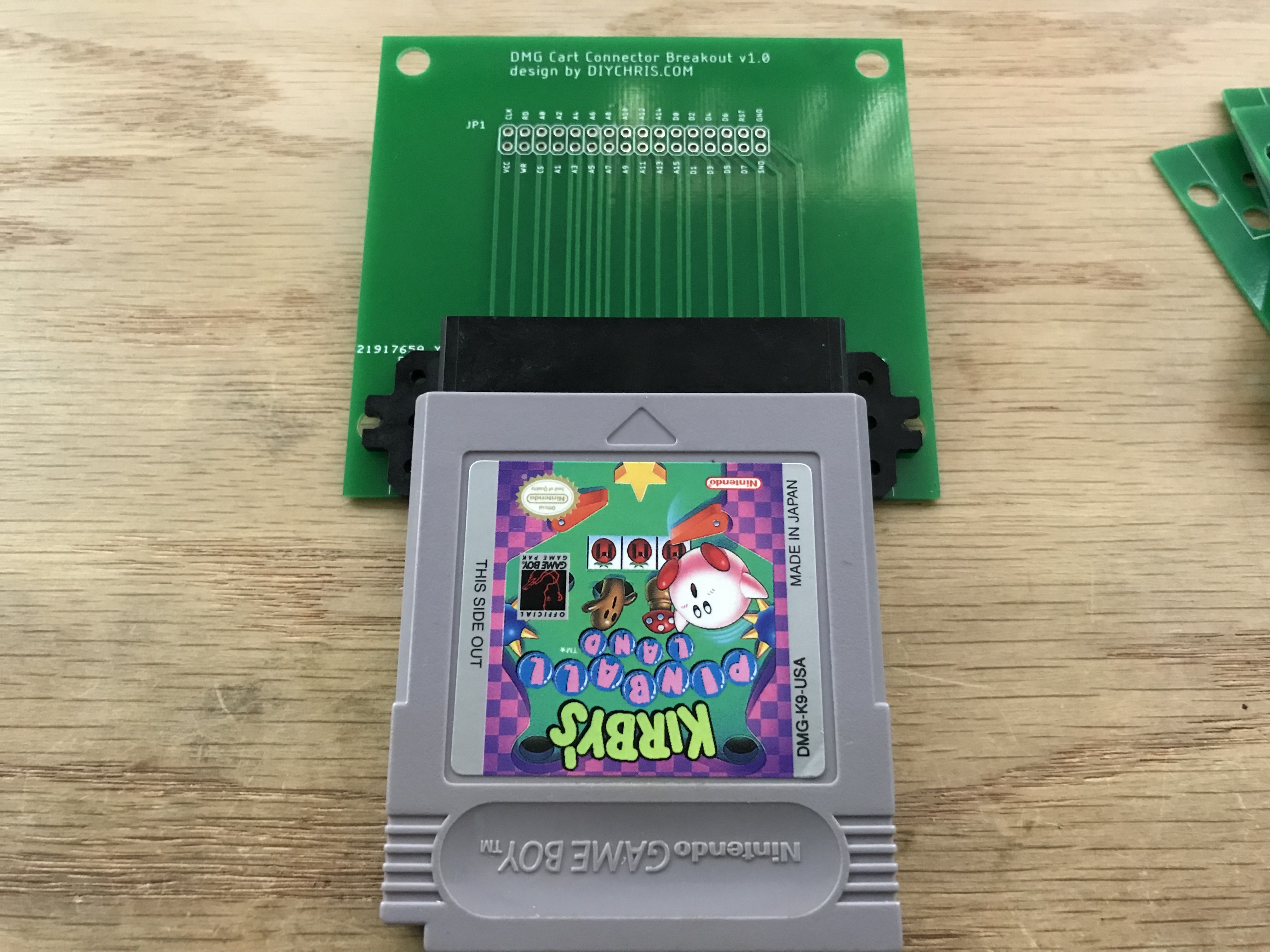
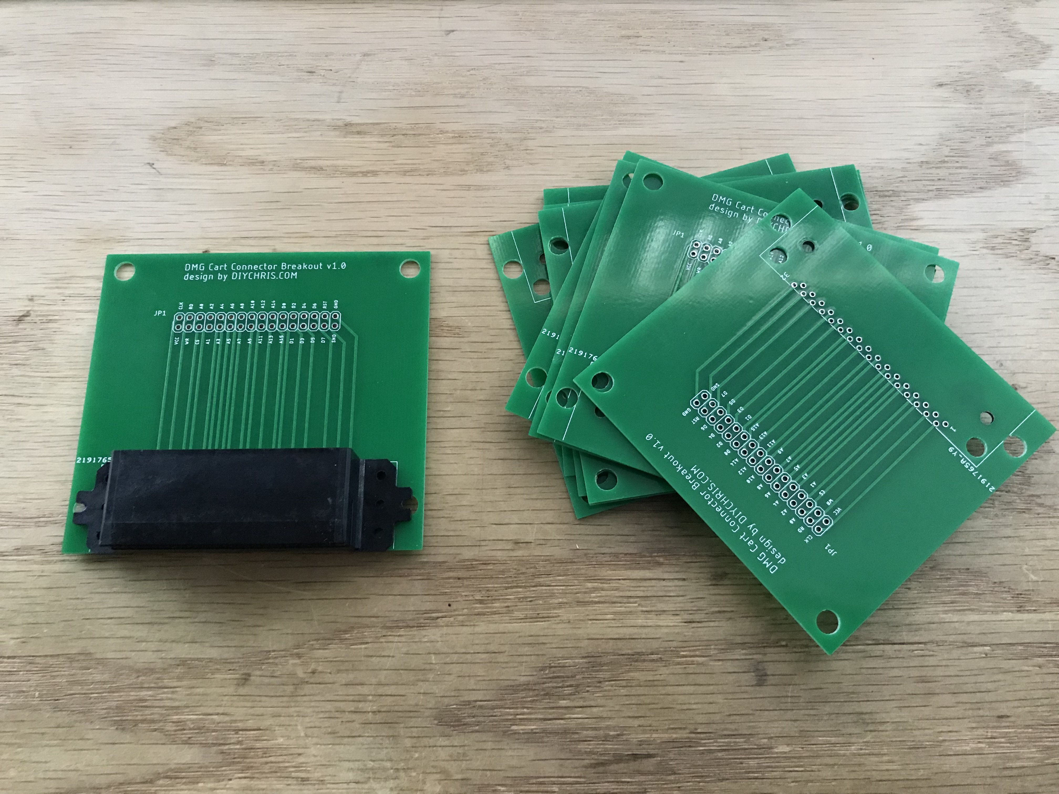
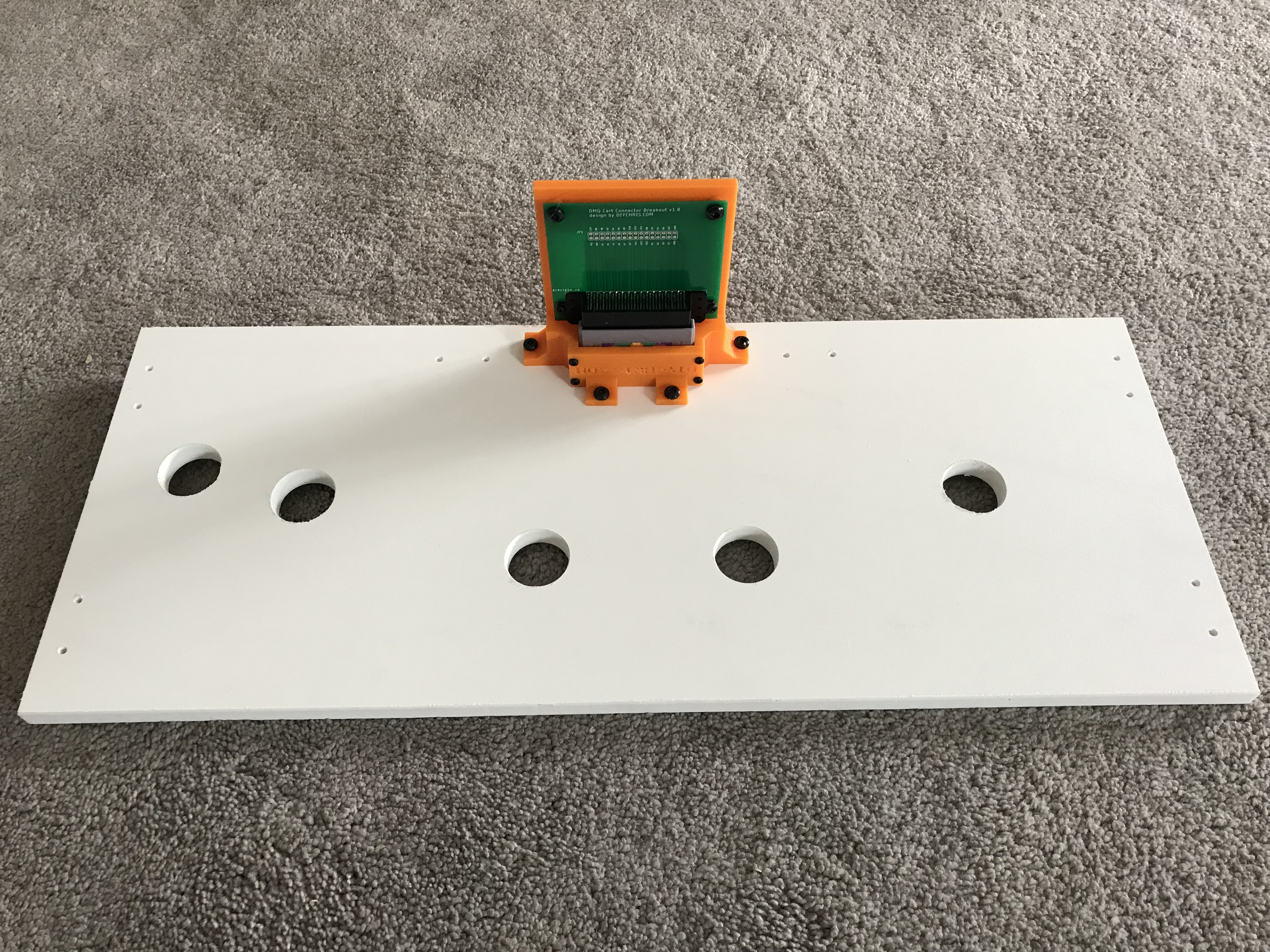
I got to thinking what might be the best way to insert the cartridge into the arcade machine to interface with the Gameboy and soon realized that I would need to remove the cartridge connector from the Gameboy’s motherboard if I wanted to have the freedom to mount it wherever I want. This is when I designed the Gameboy Cartridge Breakout Board, some pictures below:
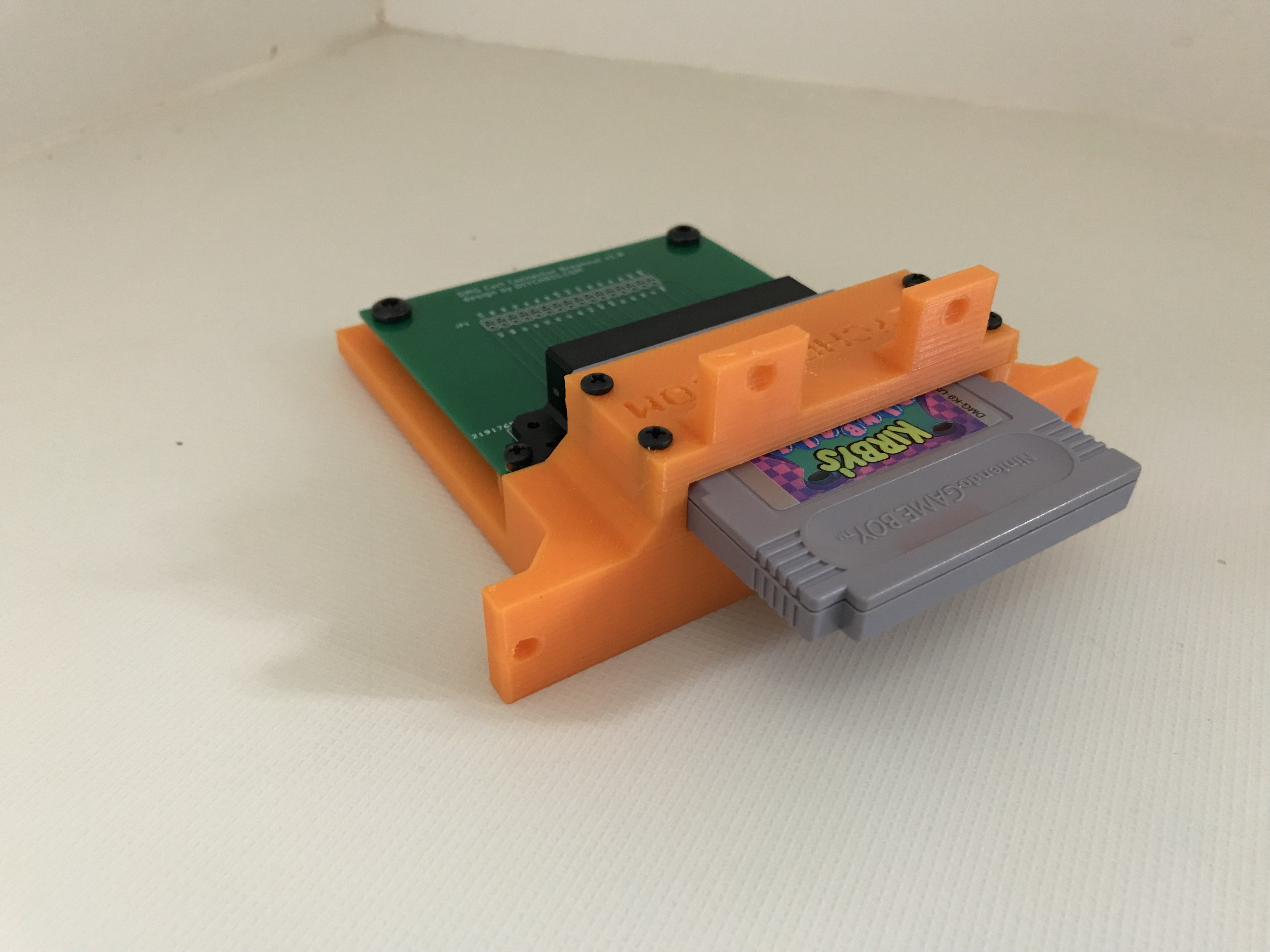
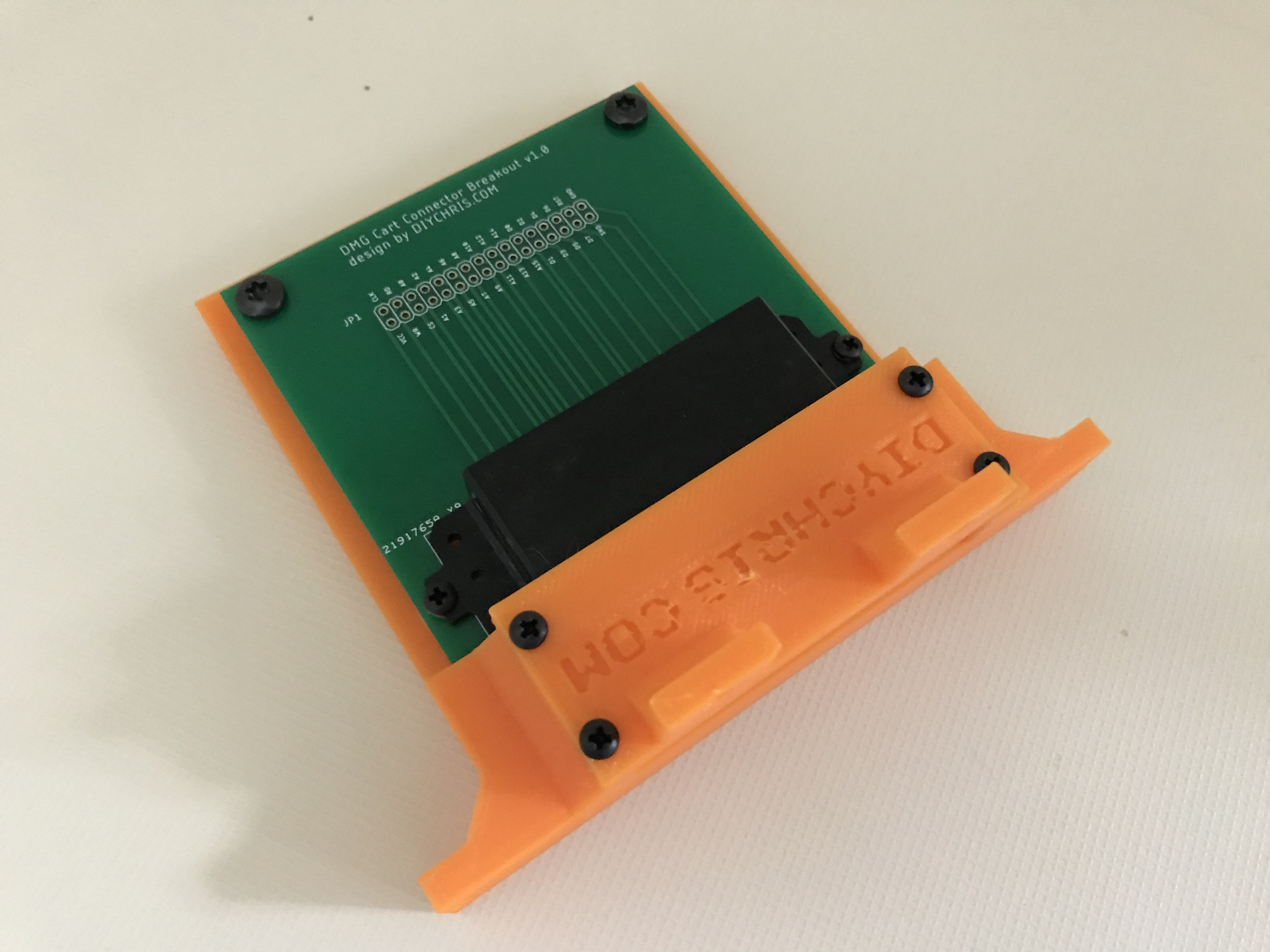
With this, I was able to design a mount and use my 3D printer to come up with this:
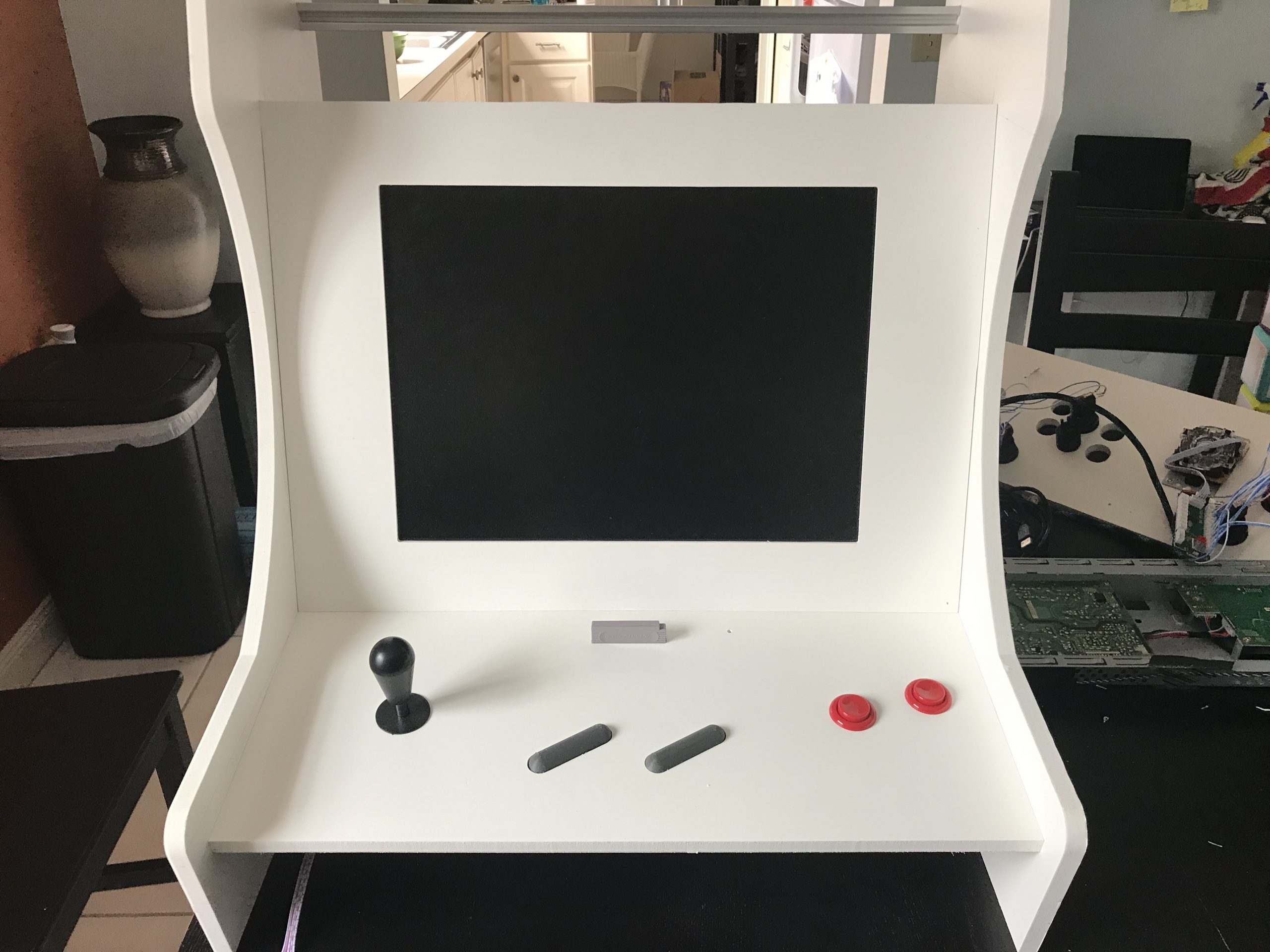
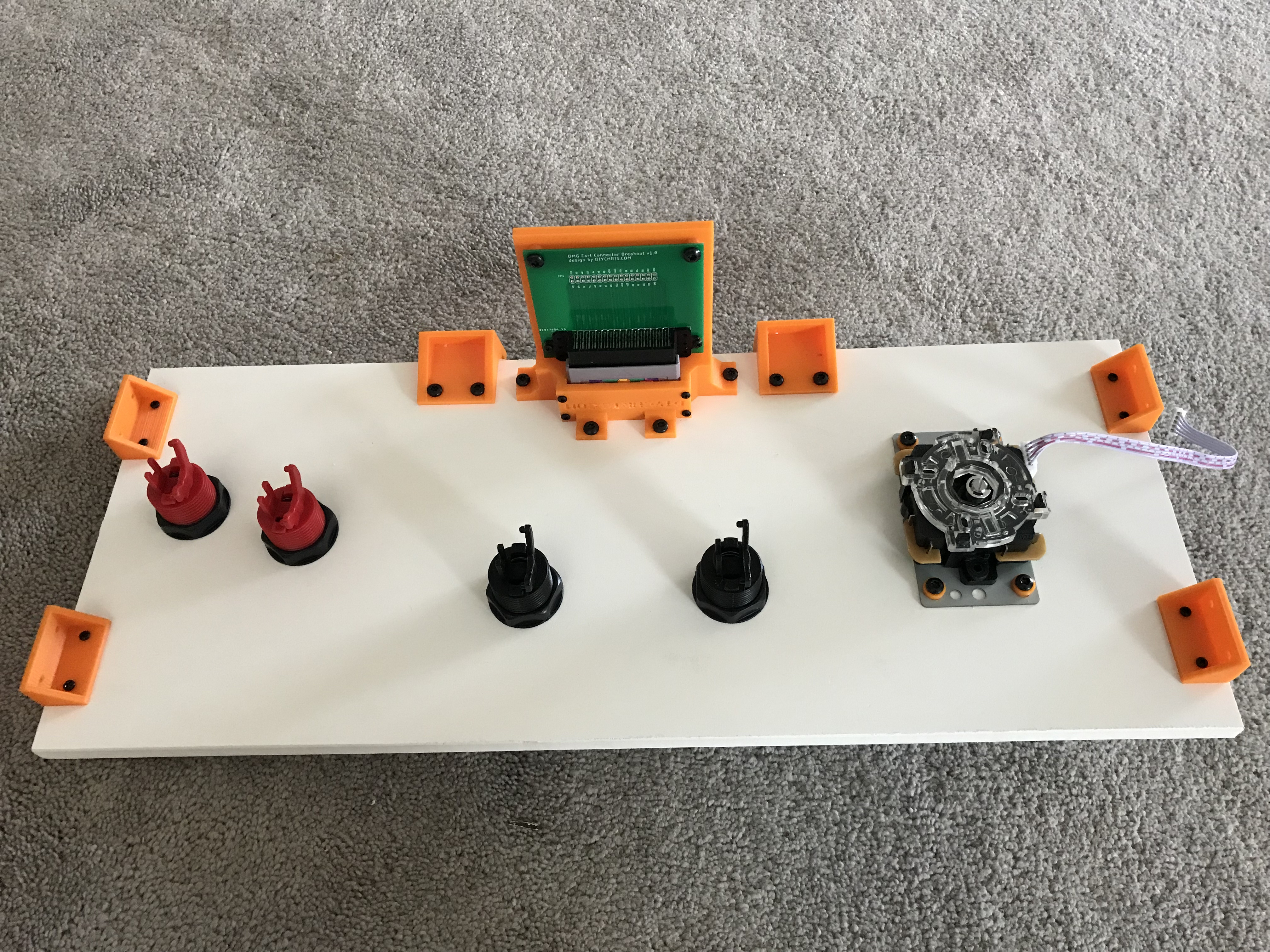
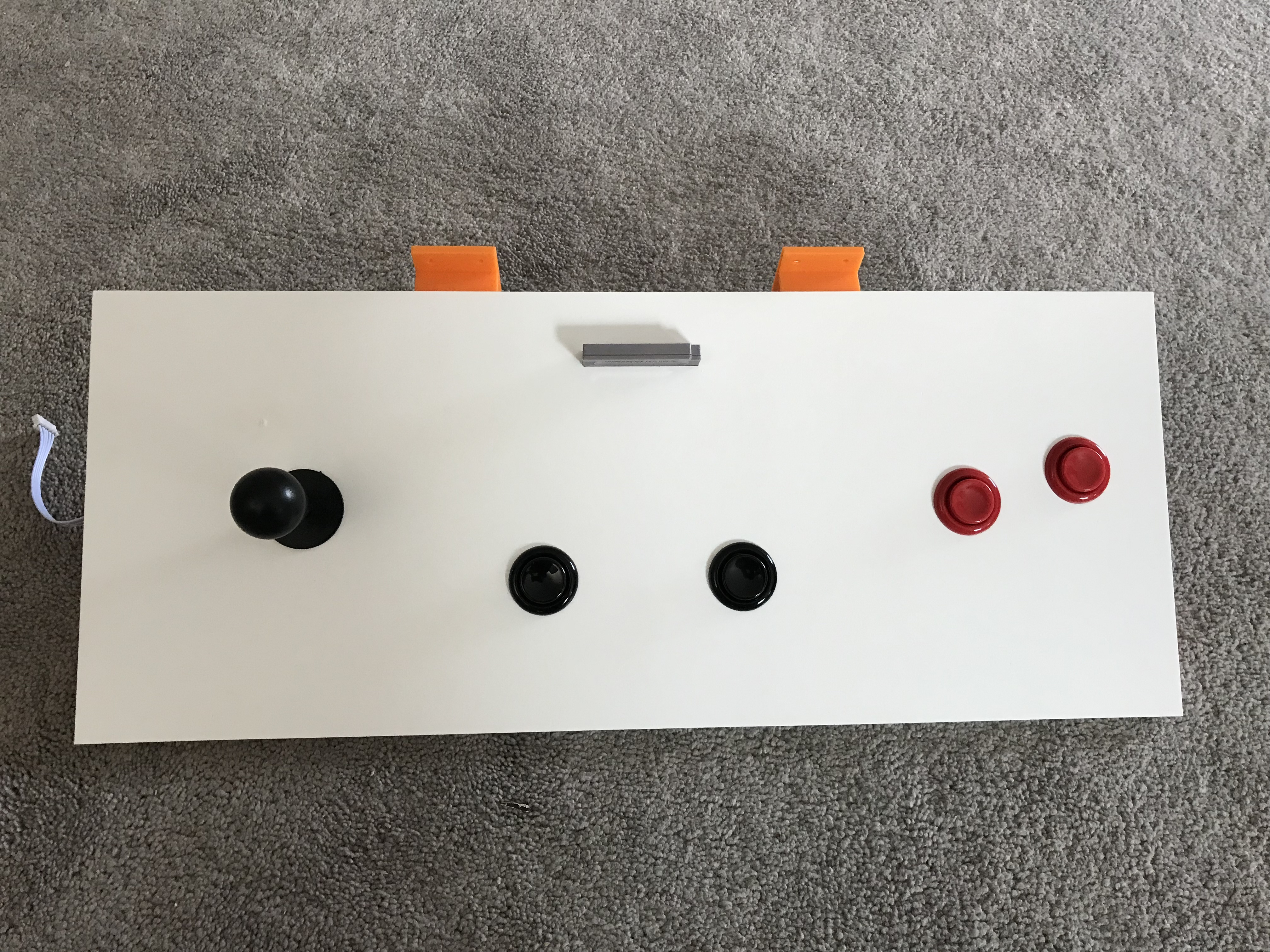
I then decided to design the main control panel for ArcadeBoy. I do all of my design work in Fusion 360 and I used my X-Carve and some 1/2 inch Sintra to carve out the panel and drill all of the mounting holes. I then attached the mount and I think it turned out pretty damn nice. I have some pictures below:
With the project moving forward at a steady pace, I decided it was time to move away from the DE0-Nano development board and try to run this thing on a dedicated FPGA. My choice for an FPGA chip was the iCE40HX1K-VQ100 based on the easyVGA module designed by uXe over at the Arduboy community and because I had some samples from way back when lying around so they were a simple choice.
I purchased some TQFP breakout boards on Amazon which are actually pretty cool, the biggest one can take anywhere from a TQFP 32 to a TQFP 100 there are also other such as SOIC which came in handy because all of the SPI Flash memory I had on hand was SOIC-8.
I soldered the FPGA onto the breakout board and then added the headers. Trying to get this to work was actually a fun little project all on its own. I started with a simple AND gate design and once I was able to successfully upload that to the SPI flash and have the FPGA configure itself, I was on to the next step which was planning out all of the pins and making all of the connections for the VGA signal along with the NES controller pins.
Here’s a picture of the worlds most complicated AND gate:
This was an accomplishing moment for me. I had spent quite a few nights and weekends trying to get all of this sorted out. Its always nice when things finally start to go your way. That just goes to show that with enough determination you can do pretty much anything. So with that out of the way, the next thing was to design the PCB for the FPGA. I did this last week and sent the designs off to a manufacturer in china. I was supposed to get the boards on Friday but the package got held up in customs so I won’t have it until tomorrow. As soon as I have my hands on them, I’ll solder everything together and test and hopefully I did everything right.
Since I wasn’t able to work on the electronics portion of ArcadeBoy this weekend, I decided to do some more work to the structure. I redesigned the controller panel, first by removing the arcade buttons for Start and Select and then by designing my own Start and Select buttons and 3D printing them. The scale is about 5.8 mm of the original Start and Select buttons. I put it together and added it to what I’ve already designed. Have a look at the pictures below:

So there it is, that’s the project so far. In hindsight, I wish I would have started documenting as soon as I started the project, this way everything would be so jumbled up but oh well, better late then never. I’ll try to update this page weekly or as updates happen which may be daily at this point.
Resources (I’ll have to eventually sort through these)
http://www.fpgalover.com/ip-cores/snes-controller-core – An IP Core for getting SNES controller inputs
http://www.fpgalover.com/attachments/article/43/SNES_FSM.v – SNES Verilog FSM
https://github.com/zephray/VerilogBoy/ – An open source FPGA compatible Gameboy
https://www.allaboutcircuits.com/projects/nes-controller-interface-with-an-arduino-uno/ – Interfacing an NES controller with an Arduino Uno (Also provides a schematic for the NES Controller)
https://community.arduboy.com/t/nes-controller-gameboy-button-translation/7183/36 – NES Gameboy Button Translation (Used this for figuring out how to interface the NES controller with the Gameboy)
https://github.com/MrBlinky/Arduboy/blob/master/SNES-controller/SNES-controller.ino – SNES Arduino
https://github.com/michael-swan?after=Y3Vyc29yOnYyOpK5MjAxNi0wMy0yOFQyMjo1NDo0MC0wNDowMM4DRlUa&tab=repositories – Useful FPGA repositories
https://learn.adafruit.com/programming-spi-flash-prom-with-an-ft232h-breakout – Programming SPI Flash with an FT232H breakout
http://www.clifford.at/icestorm/ – Open Source FPGA development tools for Windows / Linux / Mac
https://community.arduboy.com/t/vga1306-vga-out-for-diy-arduboys-implemented-on-an-fpga/4851/14 – The original thread where I discovered uXe’s easyVGA project.
https://handheldlegend.com/pages/about-us – A great source for hard to find Gameboy parts
https://sites.google.com/site/fpgaandco/de0-nano-pinout – Easier Pinout for the DE0-Nano
http://www.prismo.ch/comparisons/desktop.php – Helpful for determining screen size
http://tinyvga.com/vga-timing – Lists timing signals for different resolutions
https://lospec.com/palette-list/tag/gameboy/ – Some gameboy color palette’s
http://devrs.com/gb/files/docs.html – Gameboy technical information
https://www.t-molding.com – Great place to get everything T-Molding related