Update – 2021.06.07
Did some more work to the board over the weekend and am happy to report that we now have support for both the original PLA’s and the GAL version of the PLA. This is decided when the board is being populate. Either you solder on the 28 pin socket or the 2 24 pin sockets for the GAL chips.
Another major update is that I added RF modulator bypass circuitry so that if you choose to, you could leave the stock RF modulator disconnected and simply solder in the components for the bypass circuitry and have video out. You can also still connect the RF modulator instead.
Last but not least, I’ve added support for a wider selection of DIN connectors by adding additional pads for the shielding pins. Some more modern DIN connectors have 10mm spacing instead of 5 for the power connectors. This will make sourcing these components a bit easier.
I lied, that wasn’t last, but this is. I decided to give the project a name. The name is MELIUS. This is latin for “improved”, which I thought seemed fitting so from now on its no longer just the C64 Replica. It’s C64 MELIUS.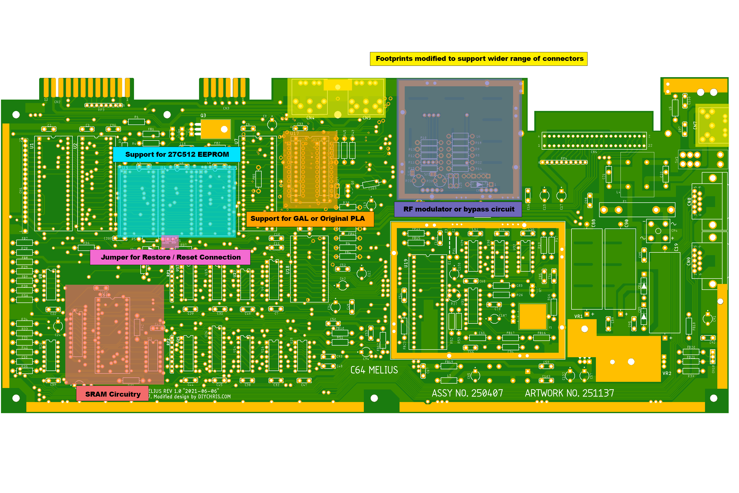
Update – 2021.06.05
There seems to be a good amount of interest so I decided to go ahead and order some boards. I’ve started allowing pre-orders for the boards. I should have them in hand by the end of next week. Lots of color options.
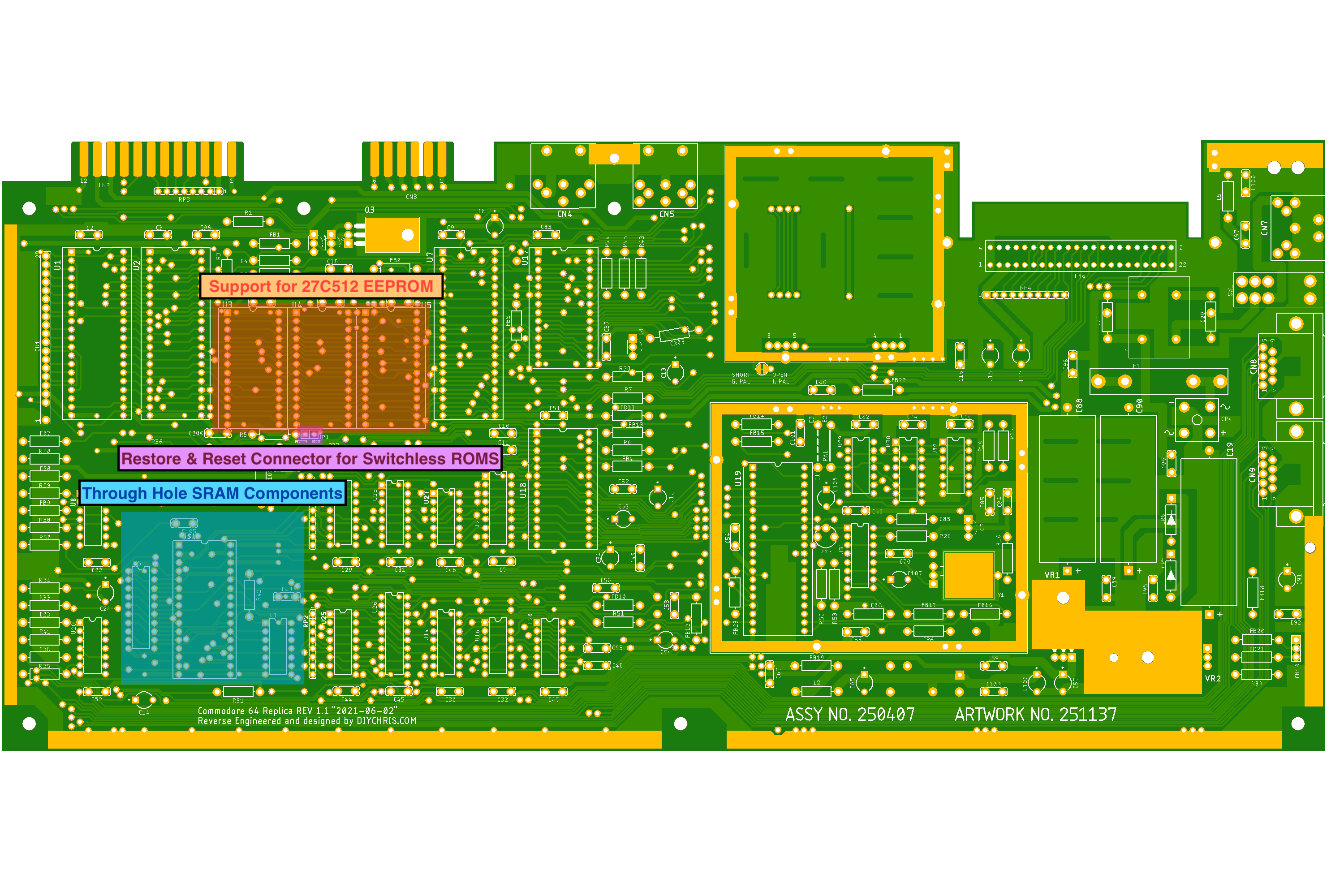
Now that I’ve got a fully working C64 replica board its time to start playing with some updates. Someone suggested that I integrate my SRAM mod directly to the board. I was skeptical at first because I built the SRAM mod using SMD components and I wanted to keep this board as simple as possible and didn’t want to have to solder on components before shipping the board. I also didn’t want to have to pay JLCPCB to add the parts for me. So after doing some research I was able to find all the required components as through hole parts. Now all I needed to do was modify the schematic and place and then route the traces. I say this as if it were quick and easy :).
So one other thing that always bothered me about all of the C64 board revisions was that you can’t just plug an EEPROM directly into the board. The ROMS commodore used were just that, ROMS. There’s a die in the center of the chip with all the logic already placed onto it at the factory. These can not be written too, only read from. So you can replace them with EEPROMs that can be written too but you have to make an adapter that reroutes the EEPROMs signal lines to match the ROM because they have 4 extra pins. I thought it would be a great mod to implement direct drop in for EEPROMs. The only downside here is that you can no longer use original ROMs. Worth it in my opinion.
Another annoyance that I though would be fun to solve is that while switchless ROMs are cool, it would be much cooler if you didn’t have to solder anything to the board when you add one. Well, you can now do this. I simply routes 2 traces to a connector that sits next to the KERNAL ROM. This gives you easy access to the /RESTORE and /RESET nets.
Here’s a picture of the mods done so far.
Update – 2021.06.03
I’m all out of the first batch of boards. Granted I only had 2 to sell because I’m a hoarder and like to keep things for myself 🙂
With that said, pre-orders are now available for Green, Black, Blue, Red or White replica boards.
https://diychris.com/index.php/product/commodore-64-250407-replica-pre-orders-available/
I don’t like doing pre-orders because I myself hate having to wait for things but its the only way for me to gauge which color boards I should order. The manufacturing process isn’t cheap and as much as I love all things Commodore I would hate to have a surplus of boards sitting around collecting dust. Although I guess you could make the argument that they would all eventually sell I just don’t have the capital to invest without knowing that they’ll sell.
I’ve set the pre-order time to be 7/6/21 which is just over a month or so but if I get enough pre-orders then I’ll definitely get these done quicker and out to you guys ASAP.
I’d like to thank everyone for supporting the project.
I’ve received some great feedback from the community and am most likely going to implement some of the requested features into future revisions of the board but it may be some time before that happens. I need a mental break for a few weeks. As I’ve said before, this was a daunting project for me and I am happy with the results and definitely feel accomplished but I don’t want to burn out.
Next will likely be a video series of me populating the board. Not sure why anyone would want to watch me do this but I’ll record it and upload it anyways.
Update – 2021.06.02
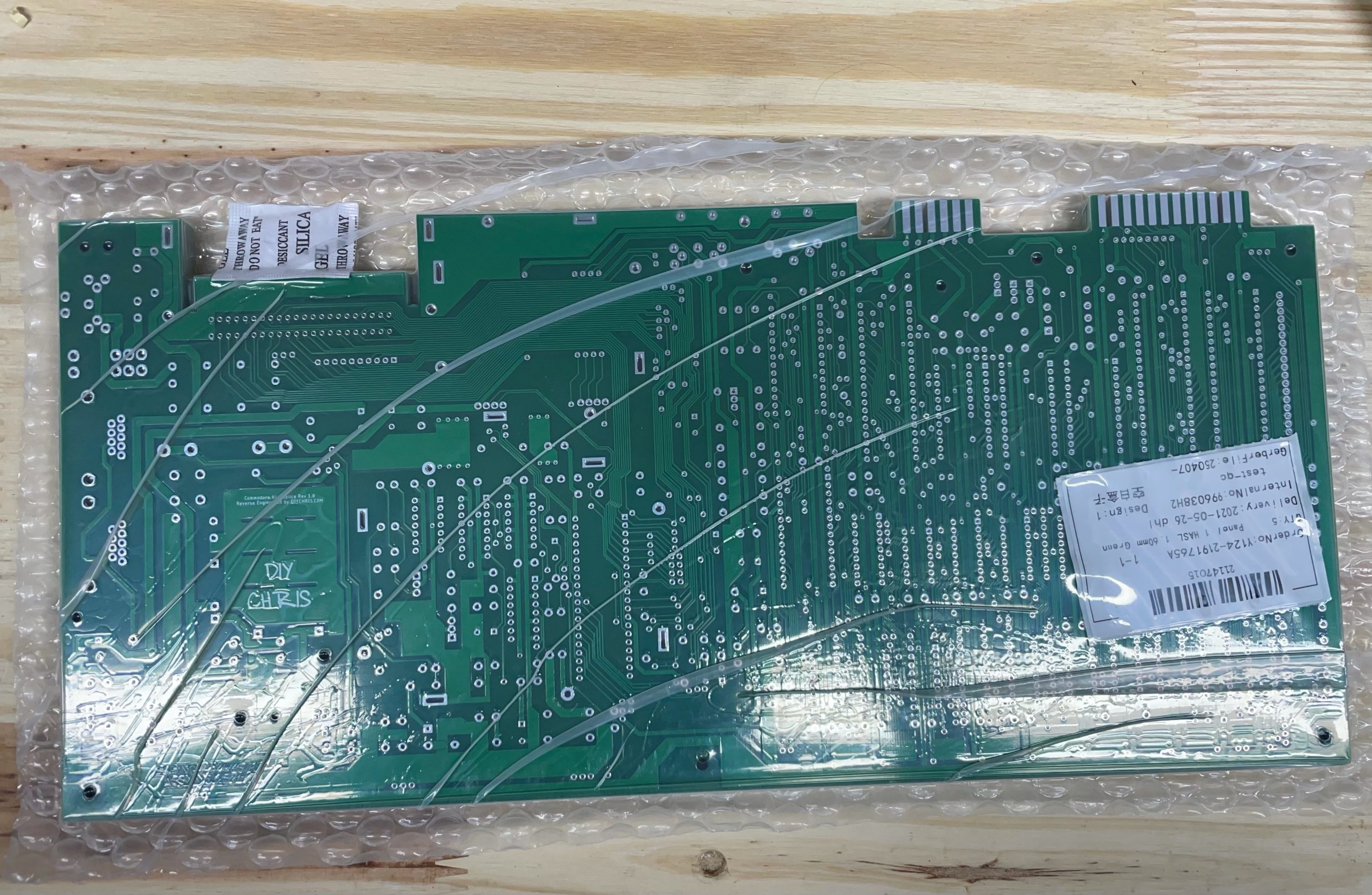
It’s a great day, I received my order from JLCPCB yesterday and got to work right away. Here’s a picture of the boards still in shrink wrap.
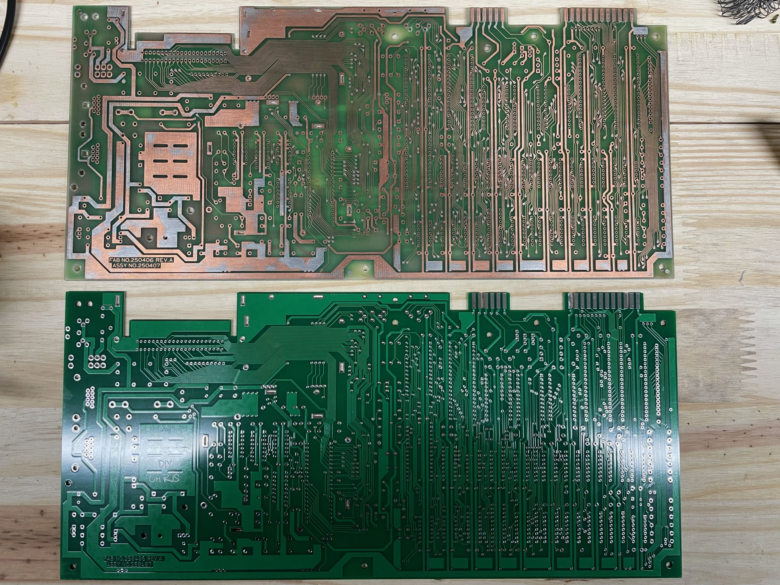
This is one of those projects that you don’t want to get into just as much as you want the satisfaction of completing it and knowing you did everything correctly for it to be 100% functional. The only way to find out for sure is to get your hands dirty and put it together. So I opened the package. For my first test I needed to check the dimensional accuracy so I took the donor board that I used to build the reference scans and compared it to the new boards. Everything lined up 100%. Below is a picture of the new and donor boards together.
Since everything checked out, it was time to get started so I started with the low profile components first (Resistors and Diodes). Here’s a picture of the resistors and diodes populated on the board.
Now it was time to put in the sockets, because I wanted to solder them all in, in a single pass I thought I’d populate all of the sockets and then flip the board over. This proved to be more difficult than initially anticipated but eventually the way I ended up doing it was to populate all of the sockets and then lay another board on top of the sockets and then flip it over on the desk and start by soldering all the corners and then coming back and checking to make sure that they were all soldered straight before finishing them up. Below is a picture of all the sockets in the board.

That was a lot of soldering and it was getting late. I didn’t want to stop here so I decided to go ahead and populate the rest of the board starting with all of the .1uF capacitors, there were so many. I then followed that up with the inductors and then the electrolytic’s followed by the RF modulator and some necessary connectors to perform my first test. Below is a picture of the board fully populated with everything you need to get a successful boot.
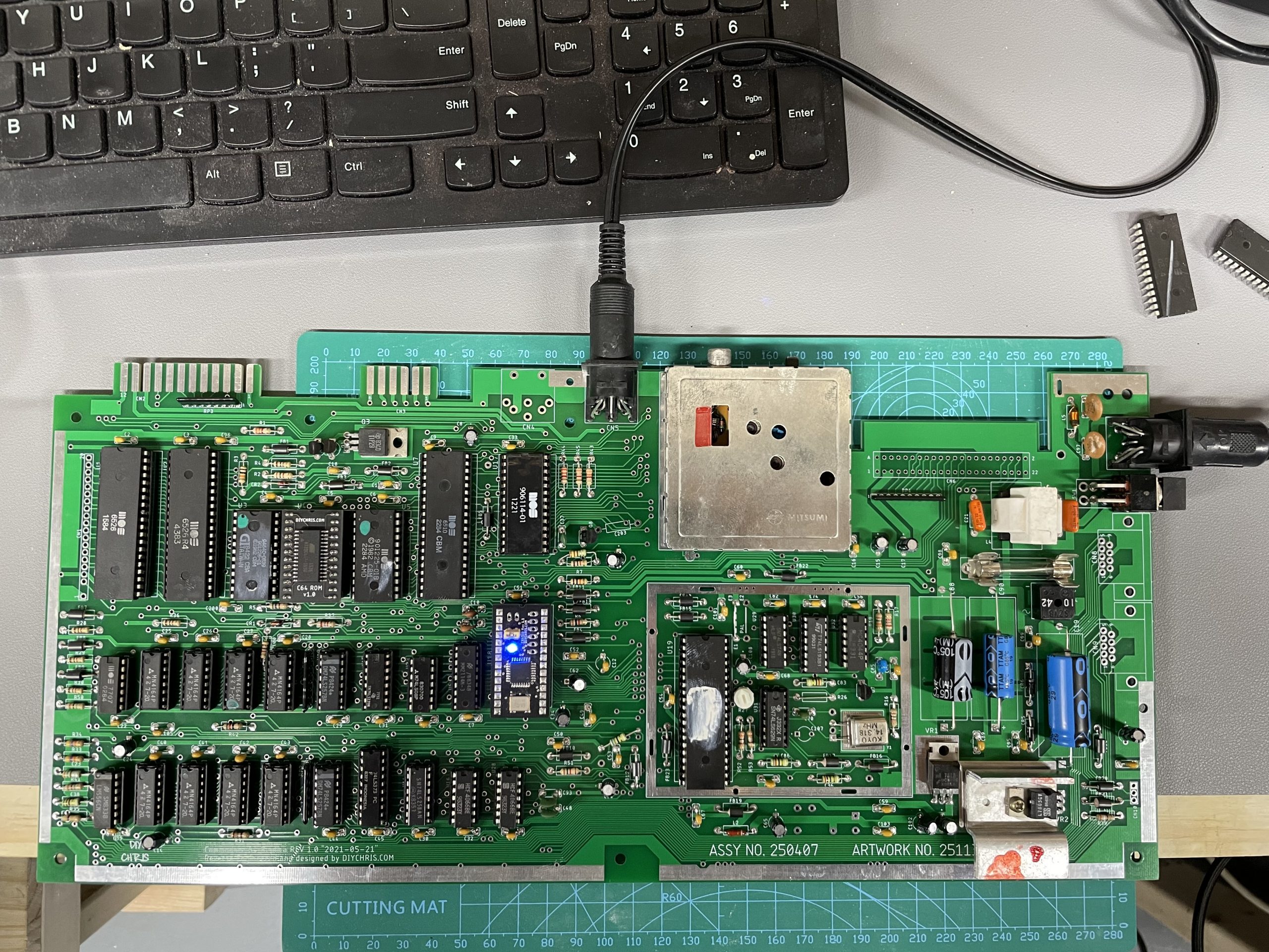
My first boot was not successful 🙁
After some troubleshooting I found that I made 2 dumb mistakes.
Mistake #1: I forgot to add FB23 which is the Ferrite Bead that connects the Phi0 output clock from the VIC chip to the CPU.. Definitely important.
Mistake #2: I forgot to add the jumper wire to select NTSC for the output.
After fixing these 2 issues the C64 came to life. I was astonished to say the least that my very first iteration of this board was a complete success with no design flaws in the schematic or board layout. I felt very pleased and extremely accomplished. There are so many things that could have gone wrong here but it all came together very nicely.
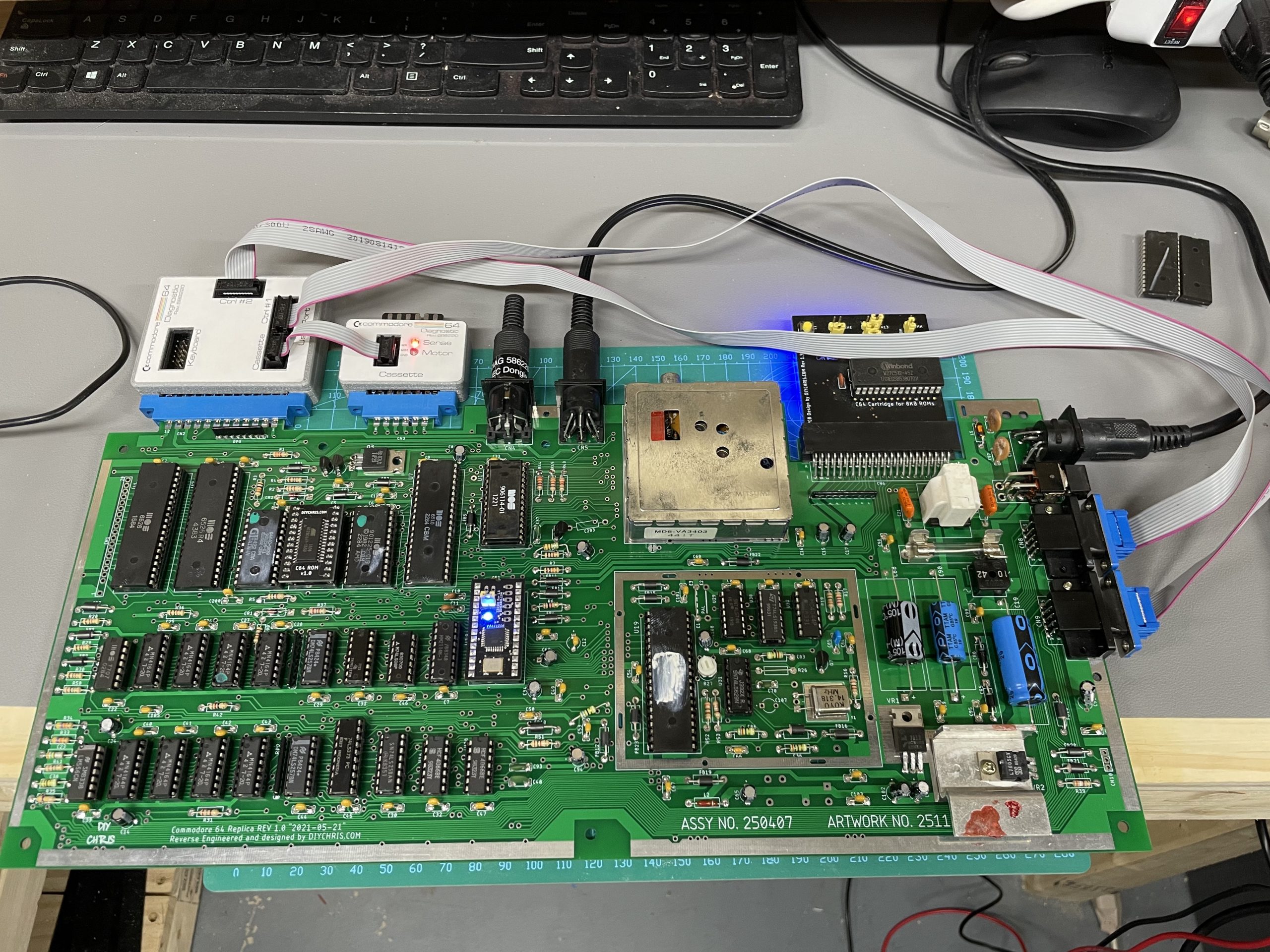
Now I wanted to test the rest of the board. Here’s some more pictures of the board with the Joystick ports, serial port and cartridge port attached.
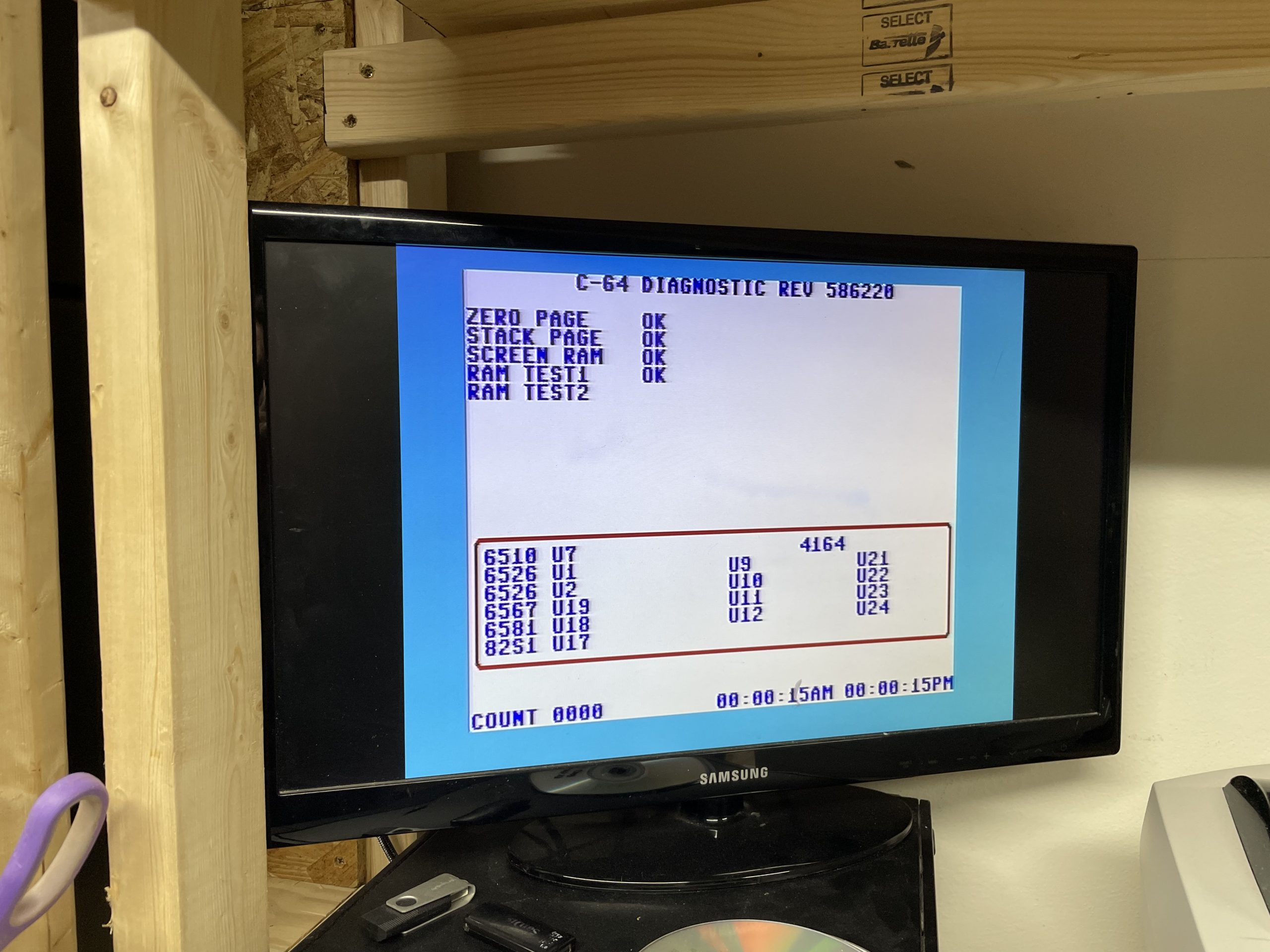
And here’s a picture of it running diagnostics
So all in all the only board layout mistakes I could find were some text that I accidentally put on the TStop layer and a wire stub that I forgot to assign to a NET. I fixed these 2 issues in Rev 1.1 which is currently sitting in my cart with JLCPCB. I gave 1 of these first ordered boards to my wife because she’s learning all about electronics and this is something she’s really excited about. I’m obviously keeping 1 or 2 for myself so that means I have at least 2 that I can sell if anyone is interested. I’ll be adding them to the store soon.
First Entry – 2021.05.22
First let me start by saying that I am aware that someone has already created a replica of the Commodore 64 250407 board and that I could easily just purchase one from him but I wanted to challenge myself to complete this project on my own from start to finish.
I’ve been wanting to create a replica of the 250407 board for quite a while now but always thought that this was going to be an overwhelming project for me to undertake. I wasn’t quite sure where to even start. I certainly wasn’t going to map out each trace on the board to create my own schematic. There are plenty of schematics floating around for the 250407 including the one in the March 1992 C64 Service Manual which is what my schematic is based on with some minor variances due to the board artwork that I was working off from.
For PCB design I like to use Autodesk Eagle, a product that I’ve been using since before it was acquired by Autodesk. So my first task was to re-create the schematic in Eagle using the schematic in the Service Manual as a guide.
Creating the schematic took a lot longer than initially anticipated. I had to create a lot of my own parts (including foot prints and symbols) to accurately represent the schematic artwork as well as the boards silk screen.
Eventually I was able to complete the schematic and so it was on to the board.
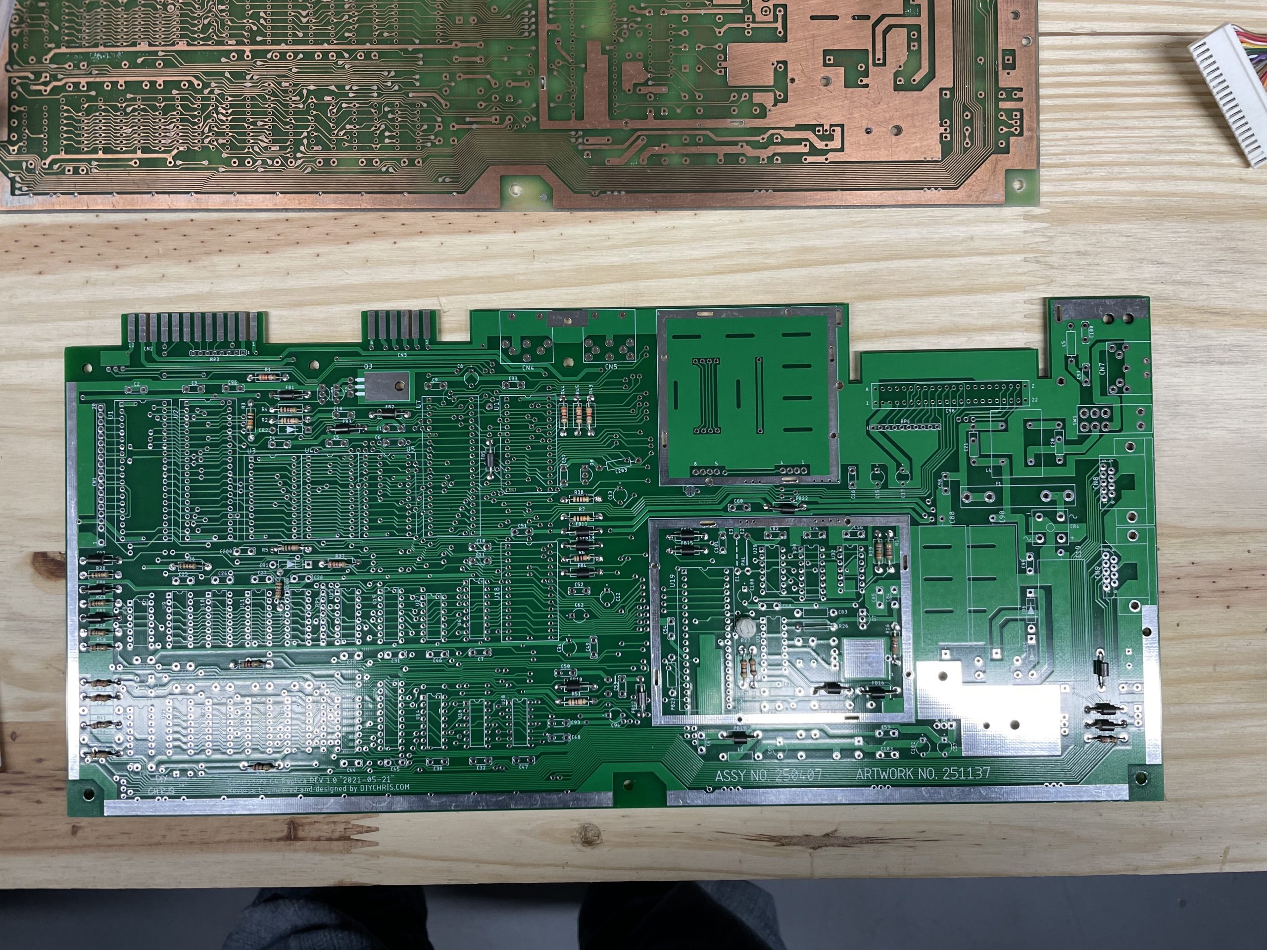
At first I was going to meticulously route all of the wires by referencing the 250407 board that I had lying around but that quickly proved to be extremely cumbersome and prone to mistakes. So what I decided to do was to sand the board down completely to expose the bare copper traces and then scan it in at a high resolution (front and back) to then further process in photoshop turning it in to a 2 color black & white bitmap.


I was then able to import this bitmap into Eagle to use as a reference for tracing the wires which made routing so much easier.
Once all the routing was complete I made some final adjustments, mainly to the tStop and bStop layers to expose the portions of the ground plane where the RF shield would be soldered. There were also several via’s that needed to be added that weren’t connected to anything, mainly to connect the ground / 5v planes between the front and back of the board.
Here are PDF’s of the final project. Currently I have the project file submitted to the PCB manufacturer and am waiting for the boards to arrive. Once they arrive, I will of course populate and test rigorously for 100% operation and if everything checks out ok I’ll sell them here on the site and maybe some other sites like eBay, Etsy, Tindie, etc…
As soon as the boards are ready I’ll post a status update here.